
Samsung Patents a Way to Fit More Light Into Each Camera Pixel
Every smartphone camera pixel needs its own set of transistors to read out light, and those transistors eat up space that could hold more light instead. Samsung's new patent describes a way to share some of those transistors across two adjacent pixels using a single bridging gate structure.
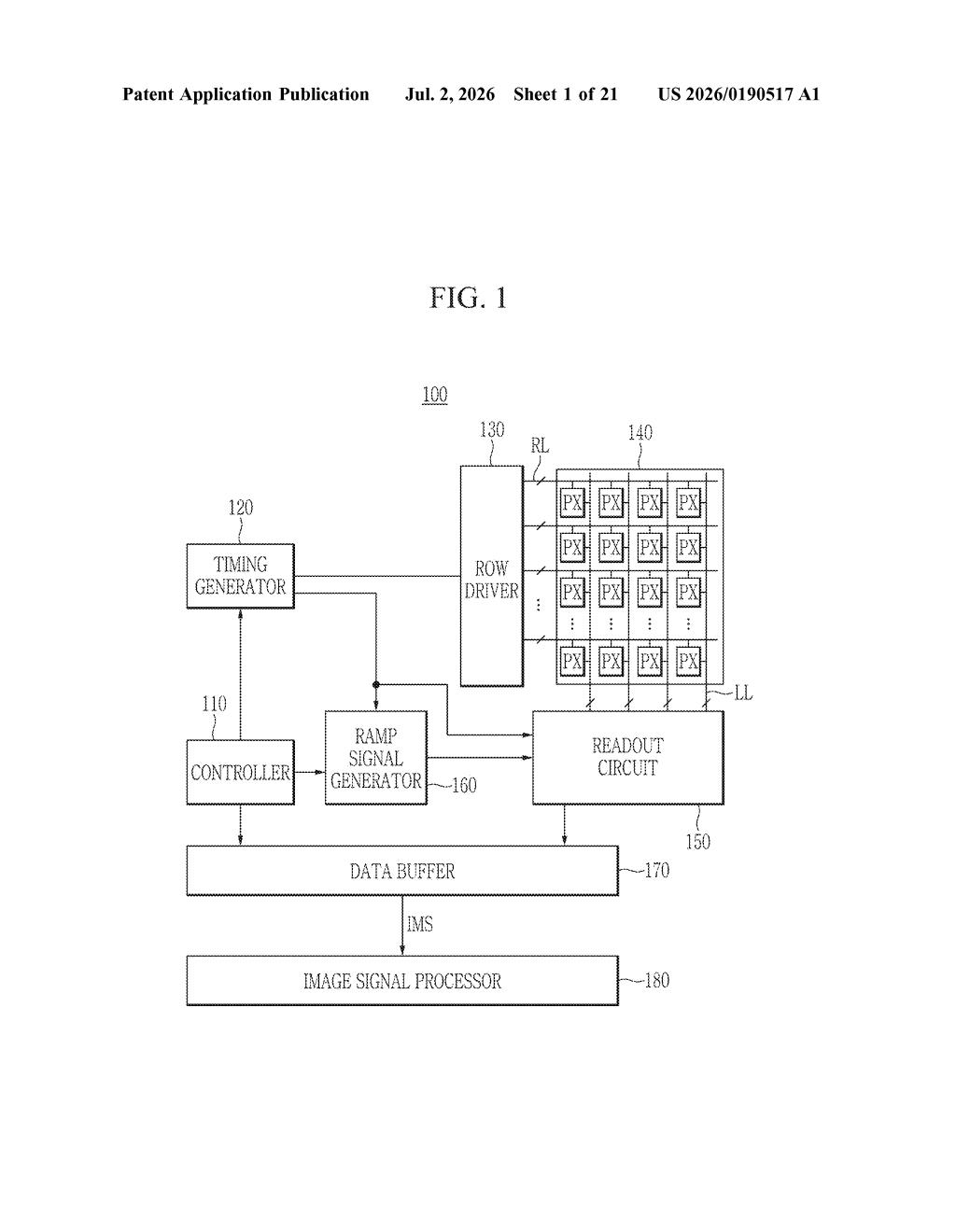
What Samsung's shared-gate image sensor actually does
Imagine each pixel in your camera sensor as a tiny bucket that collects light, with a dedicated faucet and valve to drain it for reading. Normally, every bucket needs its own set of hardware. That hardware takes up room, which means less space for the light-collecting part itself.
Samsung's patent describes a design where two neighboring pixels share some of that hardware, specifically the transistors that help read out the signal. A single gate structure, shaped a bit like a T or a bridge, reaches down into the sensor from above and connects to both pixels at once.
The practical upside is that more of the sensor's surface area can be dedicated to actually catching light, rather than to the electronics needed to process it. That tends to translate into better low-light performance and potentially sharper images from the same physical chip size.
How the dual vertical gate spans two photodiodes
The patent centers on what Samsung calls a dual vertical gate, a single electrode structure that plunges vertically into the silicon substrate and makes contact with two separate photodiodes (the light-detecting elements) simultaneously.
The gate has a top connection portion with three regions: a left zone, a right zone, and a middle zone bridging them. Two prongs, called vertical portions, extend downward from the left and right zones into the substrate. The geometry is specified precisely: the bottom of each upper zone must exactly match the width of the prong below it, and the overall bottom width of the connection portion equals the sum of all three zone widths. This tight dimensional control is what allows the structure to be reliably manufactured at scale.
Separately, the abstract describes a first active pattern that spans two adjacent photodiodes, hosting a selection gate over one pixel and a source follower gate over the other. A shared extrinsic region (a doped semiconductor zone) sits between the two pixel-separating barriers that divide those photodiodes.
- Dual vertical gate connects to two photodiodes at once
- Shared extrinsic region sits between the pixel isolation walls
- Precise width matching ensures clean electrical contacts at each prong
What this means for future Samsung camera sensors
Image sensor design has been moving toward pixel sharing for years, with companies stacking more photodiode area into the same chip footprint. Samsung already uses shared-pixel architectures in its high-resolution mobile sensors, like the ISOCELL series. This patent pushes that concept deeper into the vertical dimension, using gate structures that extend down through the silicon rather than spreading laterally.
For you as a consumer, the end goal is a camera that performs better in dim lighting without physically growing the sensor chip. Whether this specific structure makes it into a production ISOCELL sensor is unknown, but the direction is consistent with where Samsung's imaging hardware has been heading.
This is a solid incremental patent in a field Samsung clearly cares about deeply. It is not a conceptual leap, but the precise geometric constraints on the dual vertical gate suggest real engineering work toward a manufacturable solution. Pixel-sharing transistor layouts are a known path to better low-light performance, and filing detailed structural claims around a specific vertical gate geometry is exactly the kind of defensive and developmental work a leading sensor maker should be doing.
Get our take in your Top Stories
Liked this breakdown? Add Patentlyze as a preferred source on Google, and our plain-English take shows up more often in your Top Stories the next time Samsung patent news breaks.
There are more where this came from
We read every patent application Big Tech publishes and send you the ones worth knowing. Plain English, free, every week.
Want this weekly breakdown for a company we don't cover? Patentlyze Pro →