
Samsung Patents a Camera Chip Design That Reduces the Circuitry Needed to Transfer Photo Data
Moving raw pixel data off a camera sensor fast enough to keep up with modern resolution and frame rates is harder than it sounds. Samsung's new patent tries to do it with less circuitry than before.
What Samsung's shared-signal image sensor actually does
Imagine a camera sensor as a giant grid of tiny light-collecting dots. After each row of dots is read, all that raw brightness data needs to race through internal wiring to reach the processor that turns it into an actual photo. The more pixels you have, the more data needs to move, and the more wiring you need to carry it.
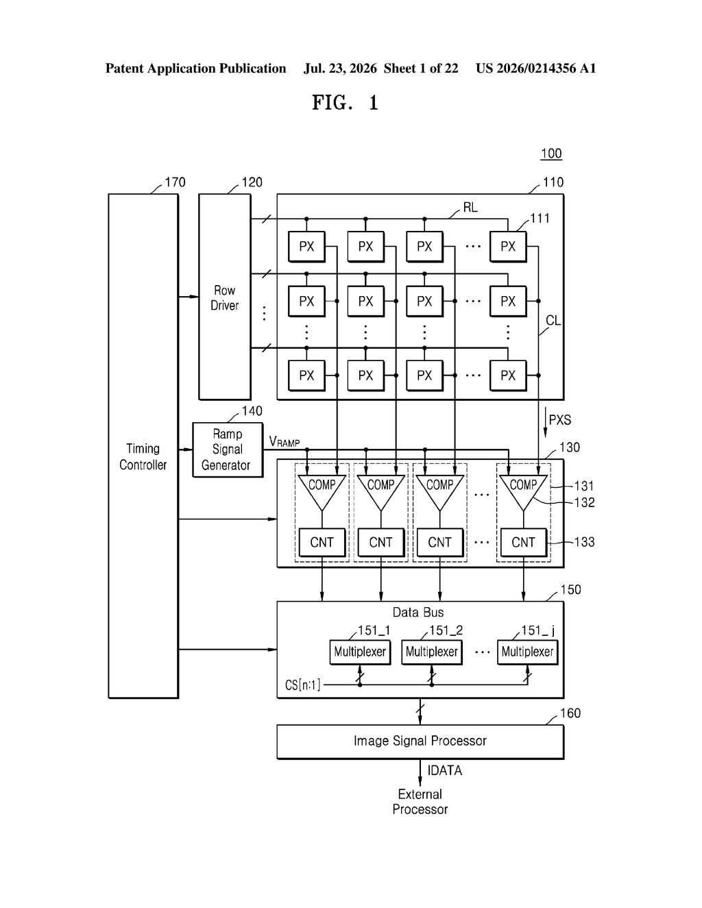
Samsung's patent describes a way to send that data using a smarter memory-and-switching arrangement inside the sensor chip itself. Instead of each output channel needing its own dedicated control wires, groups of channels share the same control signals. That cuts down on the total number of wires and logic circuits needed to shuttle data across the chip.
The end result is a cleaner, more compact internal layout that could help Samsung pack more capability into image sensors without the chip growing larger or drawing more power. It's the kind of behind-the-scenes plumbing work that rarely makes headlines but directly affects how thin a phone can be and how fast its camera can shoot.
How the multiplexer and column memory scheme works
The patent covers the internal data bus of an image sensor, which is the pathway that carries converted pixel data from the sensor array to the image signal processor (ISP), the chip that handles noise reduction, color correction, and all the other processing that turns raw data into a finished image.
Here's the architecture Samsung describes:
- Analog-to-digital converter (ADC) circuit: reads rows of pixels and converts their analog light-level signals into digital numbers.
- Channel memories: small on-chip buffers that temporarily hold pixel data. Each channel memory contains N individual column memories, each storing a different piece of pixel data.
- Multiplexers (switching circuits that choose one input from many): one per channel memory. Critically, all multiplexers across all channels share the same N selection signals rather than each having independent control lines.
By sharing selection signals, the chip avoids duplicating the control wiring for every single output channel. The first multiplexer reads through its channel memory sequentially, outputting each stored pixel value one at a time based on those shared signals. This reduces the total wire count and associated logic area on the die, which matters a great deal when you're trying to fit hundreds of output channels onto a sensor measured in millimeters.
What this means for Samsung's camera chip roadmap
Image sensors are one of Samsung's core semiconductor businesses, supplying chips to its own Galaxy phones as well as other device makers. Incremental improvements to how data moves inside these sensors directly affect resolution ceilings, frame rates, and power draw, all things that show up in camera spec sheets.
This particular patent is about die efficiency: doing the same job with less silicon area and fewer control signals. That headroom can be reinvested in higher pixel counts, faster readout speeds, or a physically smaller chip. For consumers, the downstream effect could be faster burst shooting or higher video resolutions without a battery penalty, though the patent itself is one building block among many that would need to come together for those gains to appear in an actual product.
This is quiet, foundational chip-design work, not a flashy new feature. Samsung files patents like this constantly as part of maintaining its image sensor roadmap. It matters because internal bus architecture is a real bottleneck at high resolutions, and a cleaner wiring scheme compounds over generations. Worth tracking as part of the broader picture of where Samsung's sensor division is heading, but not a story on its own.
There are more where this came from
We read every patent application Big Tech publishes and send you the ones worth knowing. Plain English, free, every week.
The drawings
22 drawing sheets from US 2026/0214356 A1 · click any drawing to enlarge


Want this weekly breakdown for a company we don't cover? Patentlyze Pro →
Be the first to weigh in