Samsung Patents a Nano-Optical Lens Layer to Sharpen Future Camera Sensors
Samsung is patenting a new way to build image sensors that uses microscopic structures — smaller than the width of a human hair — to steer light directly into each pixel, potentially capturing more light with less noise.
What Samsung's nano-lens camera sensor actually does
Picture the lens of a camera as a funnel: its whole job is to pour light onto the right spots. The pixels in your phone's camera sensor are tiny, and any light that lands in the wrong place is wasted — or worse, causes blur and noise in your photos.
Samsung's patent describes a sensor that adds a layer of nano-optical lenses — an array of extremely tiny structures — sitting right on top of the sensor's pixels. Instead of one big lens doing all the work, each pixel gets its own microscopic light-focusing structure to direct incoming light precisely where it needs to go.
Between those tiny lenses and the pixel layer, the patent adds a special material called an etch stop layer made from a transparent conductive material. This layer acts as a manufacturing safeguard, making sure the delicate nano-lenses can be built accurately without accidentally damaging the sensor underneath. It's a behind-the-scenes engineering detail, but it's what makes the ultra-precise nano-lens fabrication process practical.
How the transparent conductive etch stop layer fits in
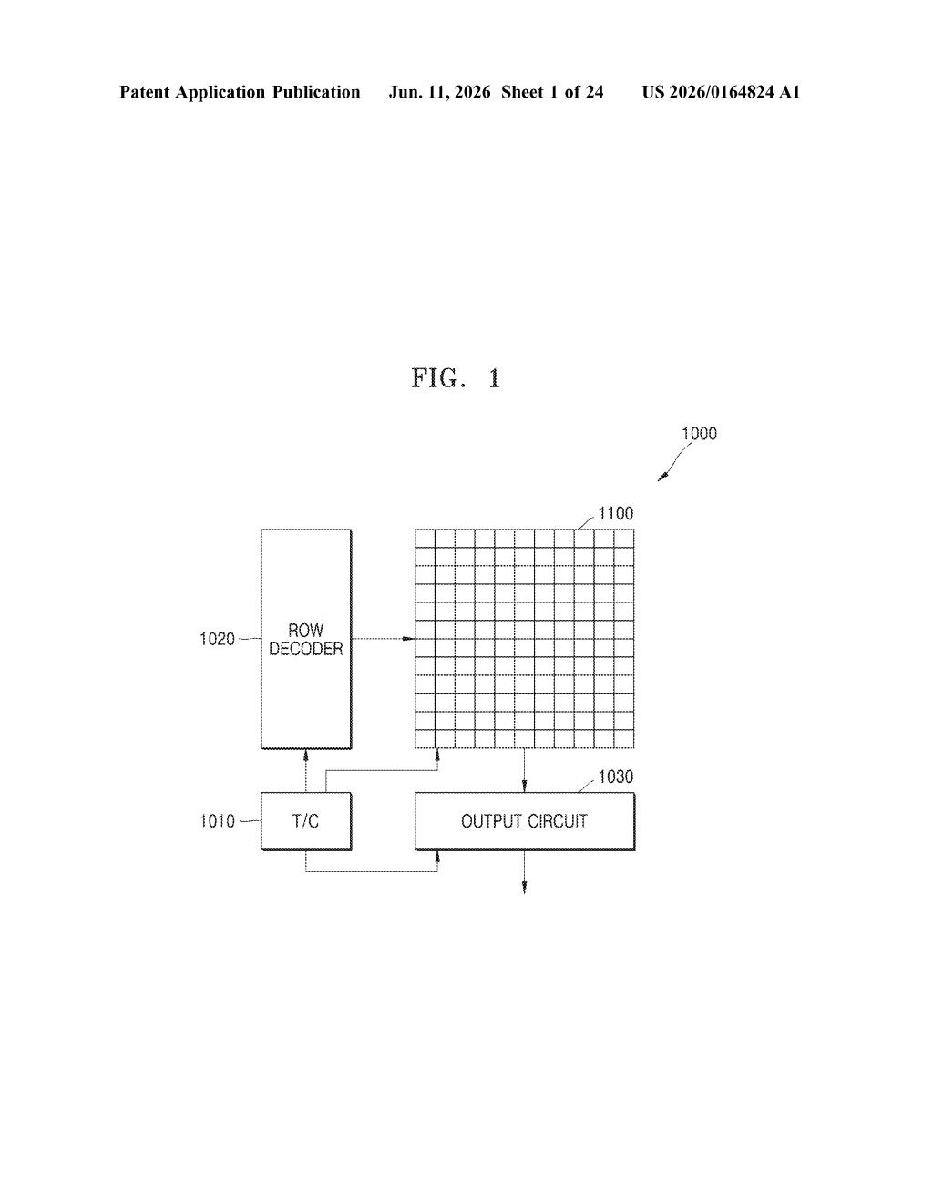
The patent describes a layered image sensor stack with four key components:
- Sensor substrate: the base layer containing the photodetectors (sensing elements) that convert light into electrical signals — the pixels themselves.
- Intermediate layer: a buffer layer sitting between the sensor substrate and the optical structures above it.
- Etch stop layer: a thin film made from a transparent conductive material (think indium tin oxide or similar compounds). In chip manufacturing, an etch stop layer tells the etching process exactly where to stop cutting — it protects underlying layers from being inadvertently damaged during fabrication.
- Nano-optical lens array: an array of nanoscale structures (features measured in nanometers — billionths of a meter) patterned to act as individual lenses, concentrating incoming photons onto specific sensing elements below.
The critical innovation is combining the etch stop function with optical transparency and conductivity. A traditional etch stop layer might block or distort light; by specifying a transparent conductive material, Samsung ensures the etch stop doesn't interfere with the light reaching the pixels while also enabling precise nano-structure patterning above it.
The net effect is more efficient light collection per pixel — particularly useful at smaller pixel sizes, where conventional lens-on-chip designs lose efficiency.
What this means for Samsung camera hardware
For smartphone cameras, the arms race has always been about squeezing more performance out of smaller pixels. As manufacturers shrink pixels to fit more of them onto a sensor, each pixel captures less light — which is why low-light photography degrades. Nano-optical lens arrays are one approach to recovering that lost efficiency by guiding light more precisely rather than just making pixels bigger.
For you as a consumer, the downstream promise is sharper low-light photos and less digital noise from Samsung's camera hardware — whether in Galaxy phones, tablets, or standalone camera modules. That said, nano-optical lens technology is still maturing, and this patent covers a specific manufacturing approach rather than a finished product.
This is a solid, incremental semiconductor patent — not a headline-grabbing AI feature, but the kind of foundational manufacturing improvement that quietly determines whether the next Galaxy camera is noticeably better in dim light. Samsung's image sensor division (ISOCELL) is a serious competitor to Sony's sensor business, and patents like this are the currency of that competition.
Get one Big Tech patent every Sunday
Plain English, intelligent commentary, no hype. Free.
Editorial commentary on a publicly published patent application. Not legal advice.