
Sony Patents a Two-Material Light Guide Design for Image Sensors
Sony is rethinking how light gets routed inside a camera sensor, and the answer involves mixing two different materials at a microscopic scale.
What Sony's two-material light guide actually does
Ever wondered why a photo taken in dim light still looks grainy, even on an expensive camera? A big part of the problem happens before the sensor even sees the light. Tiny structures inside the sensor chip are supposed to funnel each photon to exactly the right spot, and if those structures aren't working well, some light gets lost or lands in the wrong place.
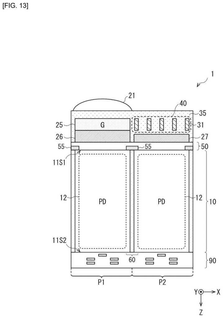
Sony's new patent describes a layer called a light guide member that sits above the actual light-sensing element in an image sensor. What's new here is that this guide is built from two different kinds of structures, each made from a different material. By pairing them together, Sony aims to steer incoming light more precisely than a single-material design could manage.
The result, in theory, is a sensor that wastes less light and delivers a cleaner image, especially in low-light situations where every photon counts. This kind of chip-level engineering is mostly invisible to you as a user, but it's the sort of change that improves every photo you take.
a first light guide member including a plurality of first structures and a plurality of second structures; and a first photoelectric conversion element that photoelectrically converts light incident through the first light guide member, wherein the first structure and the second structure include mutually different materials.
Translation: The sensor uses two different materials in its light guide to help direct incoming light to the conversion element.
How the paired structures direct light to the sensor
The core of this patent is an optical detection device, which is essentially an image sensor with a redesigned light-collection layer on top.
That layer, called the first light guide member, contains two sets of tiny physical structures built from different materials. In image sensor design, a light guide member works like a microscopic funnel array, each funnel aligned to one photoelectric conversion element (the part of the sensor that turns a photon of light into an electrical signal). When light enters from the lens, the guide is supposed to concentrate it onto those conversion elements rather than letting it scatter.
Using two different materials in alternating or paired structures gives engineers more control over how light bends and travels through the layer. Different materials have different refractive indices (basically, different abilities to bend light), so combining them lets designers shape the light path in ways a single uniform material cannot.
- First structures: one material type, likely higher or lower refractive index
- Second structures: a contrasting material, creating an optical boundary between them
- Photoelectric conversion element: receives the guided light and converts it to an electrical signal
The patent is broad at this stage, covering the general principle rather than a specific recipe for the materials involved.
An optical detection device according to one embodiment of the present disclosure includes: a first light guide member including a plurality of first structures and a plurality of second structures; and a first photoelectric conversion element that photoelectrically converts light incident through the first light guide member.
Translation: This device uses a light guide made of multiple distinct structures to channel light into a sensor.
What this means for Sony's image sensor business
Sony is one of the world's dominant image sensor manufacturers, supplying chips to Apple, Samsung, and dozens of camera makers. Any improvement at the chip architecture level, even incremental ones, ripples out across billions of devices. A more efficient light guide means sensors can be made smaller without sacrificing low-light performance, or existing sensor sizes can squeeze out better image quality.
The filing is fairly foundational in scope, which suggests Sony is staking out IP territory around a design principle rather than announcing a finished product. Sensor architecture patents like this one sit alongside a steady stream of new Big Tech patents in imaging and semiconductor optics, where the real competition happens at the microscopic level long before any camera ships.
The engineering trade here is real: mixing two materials in a microscopic structure adds manufacturing complexity and potential alignment errors that a single-material guide simply avoids. Sony is betting that the optical gain from tighter light control outweighs the production headache, and given the company's track record in sensor fabrication, that bet is probably well-placed. The risk is that the benefit narrows significantly at mass-production tolerances, where material interfaces at nanometer scales are notoriously hard to keep consistent across a wafer.
There are more where this came from
We read every patent application Big Tech publishes and send you the ones worth knowing. Plain English, free, every week.
The drawings
25 drawing sheets from US 2026/0238869 A1 · click any drawing to enlarge


Want this weekly breakdown for a company we don't cover? Patentlyze Pro →
Be the first to weigh in