
Samsung Patents a Dual-Gate Transistor Design for More Precise OLED Pixel Control
Samsung Display is rethinking how individual OLED pixels get told how bright to be — and their answer is to give the driving transistor two control gates instead of one, each fed a carefully coordinated voltage.
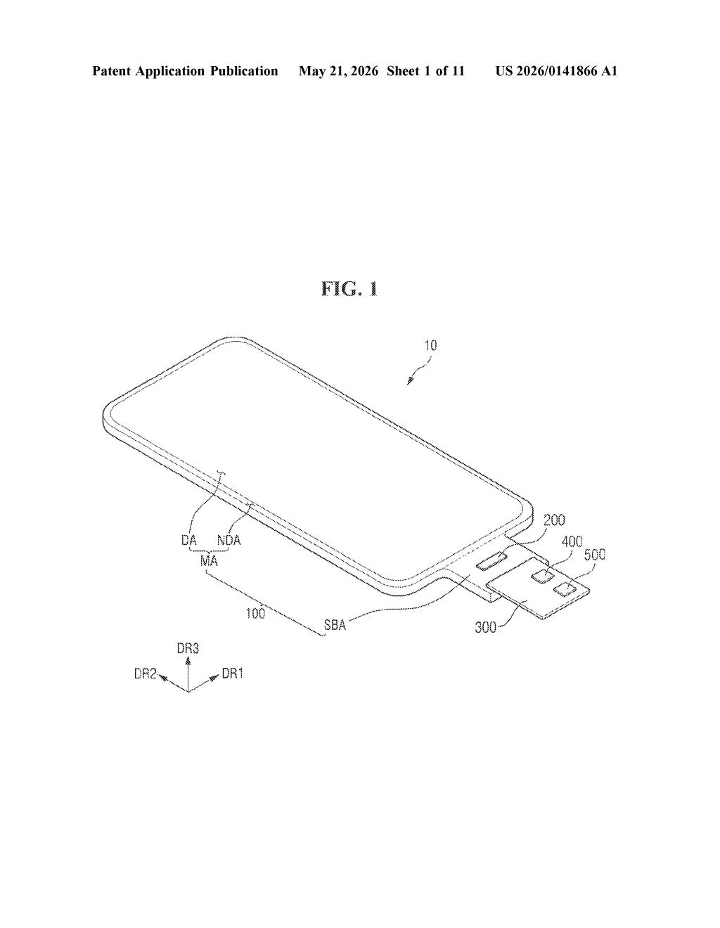
What Samsung's double-gate OLED pixel driver actually does
Imagine trying to dim a light bulb very precisely at near-zero brightness — that's one of the hardest problems in OLED display engineering. Each pixel in an OLED panel has a tiny transistor that controls how much current flows through the light-emitting layer. The brighter you want the pixel, the more current. The dimmer, the less. The problem is that at very low brightness levels, transistors behave unpredictably.
Samsung's patent describes a driving transistor with two gate electrodes — one on each side of the active semiconductor layer — instead of the usual one. Each gate is fed a separate data voltage, and the two voltages work together to control the transistor. The second voltage is derived from the first, so the driver always applies a coordinated pair.
Critically, there's a floor built in: if the first voltage drops below a certain threshold, the second voltage stops tracking it and holds steady. That prevents the transistor from entering the erratic low-signal zone, keeping dark scenes looking clean and consistent across the panel.
How the two gate voltages coordinate to drive each pixel
The core innovation is a double-gate transistor architecture for the pixel driving circuit. In a standard OLED pixel, a single-gate thin-film transistor (TFT) sits between the power supply line and the light-emitting diode. Its gate voltage — supplied by the data line — determines the current through the OLED, and therefore the pixel's brightness.
Here, Samsung replaces that single-gate transistor with one that has two gate electrodes facing each other, sandwiching the active semiconductor layer in between. A first data line feeds the top gate and a second data line feeds the bottom gate, both driven by the same data driver IC.
The data driver sends a first data voltage down the primary line and a second data voltage — always a different magnitude — down the secondary line. Crucially, the second voltage is a function of the first: the driver calculates or looks up the companion voltage based on whatever brightness level the first voltage encodes.
The claim also specifies a lower-limit clamp: if the first data voltage dips below a defined floor, the second voltage freezes at the value it would have had at that floor rather than continuing to track downward. This prevents both gates from simultaneously pushing the transistor into an unreliable operating region at near-black brightness levels, which is a known weak spot for OLED pixel circuits.
What this means for OLED display uniformity and low-brightness accuracy
OLED displays already have a reputation for deep blacks, but near-black uniformity — where tiny current variations cause visible banding or mura across the panel — is a persistent manufacturing headache. By using two coordinated gate voltages, Samsung's approach effectively widens the transistor's usable control range and reduces sensitivity to process variation in the thin-film layer. You'd most likely notice the difference in dark cinematic scenes or always-on watch faces where low-luminance accuracy is everything.
The lower-limit clamping behavior is the detail worth watching. It's a deliberate circuit-level safeguard that keeps pixel drivers out of a noisy operating zone — the kind of engineering that shows up in premium panels targeting HDR accuracy. Whether this appears in Galaxy phones, QD-OLED TVs, or foldable displays isn't specified, but all three product lines would benefit.
This is a solid, specific display engineering patent — not a broad platform claim, but a well-defined circuit technique for a real problem. The dual-gate TFT idea itself isn't new to semiconductor physics, but applying it with a coordinated companion voltage and a hard clamp at the low end is a practical, manufacturable take on fixing OLED dark-scene quality. Worth tracking if you follow display panel technology.
Get our take in your Top Stories
Liked this breakdown? Add Patentlyze as a preferred source on Google, and our plain-English take shows up more often in your Top Stories the next time Samsung patent news breaks.
There are more where this came from
We read every patent application Big Tech publishes and send you the ones worth knowing. Plain English, free, every week.
Want this weekly breakdown for a company we don't cover? Patentlyze Pro →