Qualcomm Patents a Memory System That Computes and Transfers Data at the Same Time
Moving data between memory and a processor is one of the biggest bottlenecks in modern chips. Qualcomm's new patent describes a memory architecture that sidesteps that bottleneck by doing computation directly inside the RAM — while normal memory traffic keeps flowing uninterrupted.
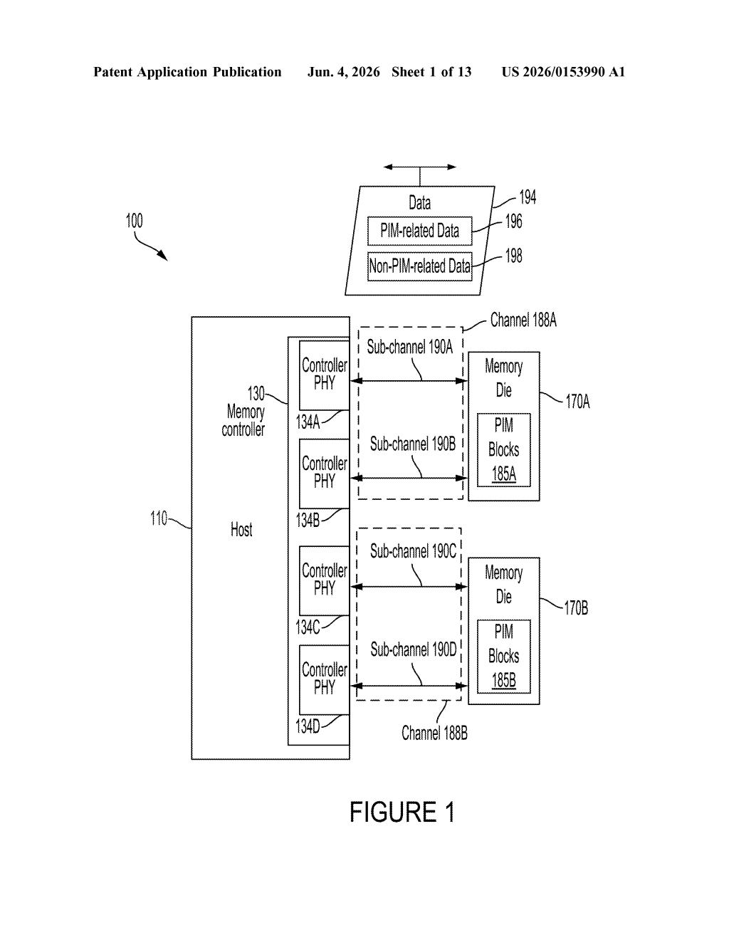
What Qualcomm's split-channel PIM memory actually does
Imagine a busy kitchen where one cook is plating finished dishes while another is still chopping vegetables in the back. They're not blocking each other — work is happening in parallel. That's roughly the idea behind Qualcomm's new memory patent.
Normally, when a chip needs to crunch numbers, it has to pull data out of memory, do the math on a separate processor, then push results back. All that shuttling takes time and energy. Processor-in-Memory (PIM) is a design approach that puts small compute units inside the memory chips themselves, so calculations can happen right where the data lives.
Qualcomm's twist is splitting the memory into two lanes. One lane handles regular read/write traffic between your app and the chip. The other lane quietly runs its own PIM computations in the background, with its external communication port turned off so it doesn't interfere. You get both jobs done at the same time, without one stalling the other.
How Qualcomm divides memory channels to hide compute latency
The patent describes a memory system with two sub-channel interfaces — think of them as two separate communication lanes into the same memory chip.
- Sub-channel 1 stays active and handles standard memory access commands — reads, writes, and similar traffic flowing between the host processor and the first group of memory banks.
- Sub-channel 2 is disabled on the external side during this mode, meaning no host traffic flows through it. Instead, the PIM blocks attached to the second group of memory banks run their own compute operations independently.
- Both sides operate concurrently — the host doesn't have to wait for the PIM work to finish, and the PIM work isn't interrupted by host memory requests.
PIM (Processor-in-Memory) is a hardware design where small processors are integrated directly into a memory die, letting computation happen close to the data rather than shipping data across a bus to a central CPU or GPU. This dramatically cuts the energy and latency cost of memory-bound workloads.
The key architectural insight here is the controlled disabling of the second sub-channel interface. By shutting off that external port during PIM operation, Qualcomm avoids bus contention (two things fighting over the same communication line) and keeps both workstreams cleanly isolated.
What this means for AI chips and mobile processing
Memory bandwidth is increasingly the limiting factor in AI inference and other data-heavy workloads — especially on mobile and edge devices where you can't just throw more cooling and power at the problem. A design that lets PIM compute run in the background without stealing bandwidth from normal memory traffic could meaningfully improve throughput per watt, which is exactly the metric that matters most in Qualcomm's core markets.
For on-device AI specifically — running large language model layers or neural network inference locally on a phone or PC chip — this kind of architecture could allow more compute to happen in parallel without the usual penalty of saturating the memory bus. It's the kind of low-level plumbing work that rarely makes headlines but directly affects how fast your AI features run and how long your battery lasts.
This is serious chip architecture work, not a novelty filing. The specific mechanism — cleanly partitioning memory channels so PIM and host access don't collide — addresses a real and well-documented problem in memory-bound AI workloads. Qualcomm is clearly thinking hard about where the bottlenecks will be in next-generation on-device AI silicon, and this patent reflects that.
Get one Big Tech patent every Sunday
Plain English, intelligent commentary, no hype. Free.
Editorial commentary on a publicly published patent application. Not legal advice.