
Samsung Patents an Optical Waveguide Design That Controls How Light Bounces Through AR Lenses
Getting light to travel cleanly through a thin lens is one of the hardest manufacturing problems in AR glasses. Samsung's latest patent takes a careful look at the surfaces that light bounces off, and tries to control exactly how rough they are.
What Samsung's matched-surface waveguide actually does
Imagine a tiny glass highway built into the lens of a pair of AR glasses. Light enters at one end, bounces along the inside, and exits where the display needs it. If the walls of that highway are uneven, light scatters in the wrong directions and the image you see looks blurry or washed out.
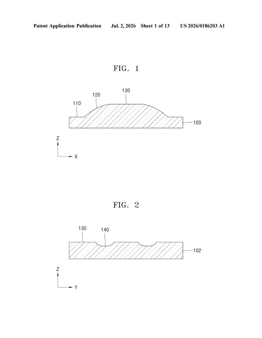
Samsung's patent describes an optical waveguide, the thin transparent slab that guides light in AR headsets, with a specific three-surface shape. Two of those surfaces, the ones light actually travels along, are manufactured to have exactly the same roughness level. That consistency is harder to achieve than it sounds, because different manufacturing steps can leave different textures on different faces.
By locking those two surfaces to the same roughness, Samsung aims to keep light behaving predictably as it travels through the waveguide. The practical goal is cleaner, more consistent images in whatever display product this ends up inside.
How the three-face geometry keeps light on track
The patent describes an optical waveguide with three distinct faces arranged in a stepped geometry. The first face and second face are connected to each other, and the third face sits at a different height (in what the patent calls the "first direction") than the first face, making it the topmost surface.
The key technical claim is that the surface roughness (a measure of microscopic bumps and valleys on a surface, usually expressed in nanometers) of the first face equals the surface roughness of the second face. In optical components, roughness matters because even tiny surface irregularities scatter light, causing signal loss or image artifacts.
- The stepped, three-face profile suggests this waveguide is shaped for a specific coupling or exit point, common in diffractive waveguide designs used in AR optics.
- Matching roughness across two faces implies the patent covers a manufacturing process, not just geometry, since achieving equal roughness on surfaces formed by different cutting or etching steps requires careful process control.
- The USPC classification 385/14 places this squarely in optical waveguides, consistent with AR display components.
The patent is relatively narrow in scope, focused on this surface-matching property rather than a full waveguide system.
What this means for Samsung's AR glasses ambitions
For AR glasses, waveguide quality is one of the biggest barriers between a lab prototype and a product people actually want to wear. Light loss and scattering inside the waveguide directly degrade image brightness and clarity. A manufacturing approach that ensures consistent surface roughness across multiple faces could reduce defect rates and improve yield, which matters enormously when you are trying to make millions of units.
Samsung has been widely reported to be working on AR glasses to compete with products from Meta and Apple. A filing like this, focused on the precision manufacturing details of a core optical component, fits the kind of foundational IP work a company does before it announces a consumer product. It does not confirm a specific product, but it does confirm that Samsung's optics team is working at a detailed manufacturing level.
This is a narrow, incremental manufacturing patent, not a headline feature. Surface roughness matching on a waveguide is the kind of detail that only matters if you are actually building AR lenses at scale, which is exactly what makes it worth a second look. Samsung is doing the unglamorous precision work that separates companies that ship AR products from companies that demo them.
Get our take in your Top Stories
Liked this breakdown? Add Patentlyze as a preferred source on Google, and our plain-English take shows up more often in your Top Stories the next time Samsung patent news breaks.
There are more where this came from
We read every patent application Big Tech publishes and send you the ones worth knowing. Plain English, free, every week.
Want this weekly breakdown for a company we don't cover? Patentlyze Pro →