
Qualcomm Patent Automates 3D Texture Resolution Decisions Through Dicing Oracle Technology
Every time a GPU renders a 3D scene, it has to make constant guesses about how much texture detail to actually draw. Qualcomm has filed a patent for a system that takes that guesswork away automatically.
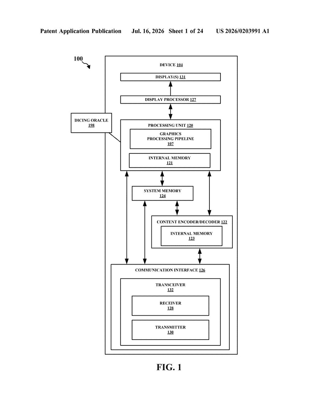
What Qualcomm's texture resolution system actually does
Imagine a video game rendering a detailed stone wall. When that wall is far away, you don't need every pore and crack rendered in full detail, the player can't see them anyway. But the GPU still has to decide, in real time, how much detail to bother with at any given distance and angle. Get it wrong and you either waste processing power or end up with blurry, low-quality textures.
Qualcomm's patent describes a system called a "dicing oracle" that figures out the right level of texture detail automatically. It looks at how an object is positioned on screen, calculates how its surface maps to actual pixels, and then picks the correct resolution for the texture data used in rendering.
The goal is efficiency: stop rendering more detail than what's visible, and stop rendering too little. This kind of optimization matters most in devices where every bit of processing power counts, like smartphones and standalone VR headsets.
How the mip region map resolution gets calculated
The patent describes a system built around what's called texture space shading, a rendering technique where shading calculations happen in a separate coordinate space (mapped to the object's surface) rather than directly on screen pixels. That separation can improve efficiency, but it introduces a problem: how do you know how much resolution you actually need in that separate texture space?
Here's how the system works:
- The processor takes a 3D object broken into small mesh chunks called meshlets and maps them using UV coordinates (a 2D grid that wraps around the 3D surface like a flattened skin).
- It renders those meshlets to figure out how they land on the actual screen, then calculates derivatives (rates of change in the UV mapping, which tell you how much the texture stretches or compresses at any point).
- Using those derivatives and a target pixel density, it calculates the ideal resolution for a mip region map (a pre-computed set of texture detail levels, where "mip" stands for the Latin phrase meaning "many things in a small place").
The output is a specific resolution value that downstream rendering steps use to load exactly the right amount of texture detail, no more and no less.
What this means for mobile and chip-level graphics
For Qualcomm, which makes the Snapdragon chips inside most high-end Android phones and several standalone VR headsets, squeezing better graphics out of a constrained power budget is a core competitive concern. A system that automatically matches texture resolution to what's actually visible on screen could reduce GPU load without any drop in perceived image quality.
This is particularly relevant as mobile games push closer to console-quality graphics and as standalone VR devices try to render complex 3D scenes without a tethered PC. Wasting GPU cycles on texture detail nobody sees is a real cost in battery life and heat, and this patent targets exactly that waste.
This is a focused, practical patent aimed at a real inefficiency in GPU rendering pipelines. It's not a flashy AI play or a new product category, it's the kind of unglamorous optimization work that actually makes graphics chips faster and cooler. For anyone watching Qualcomm's push into high-performance mobile and XR graphics, it's a meaningful signal about where their engineering attention is going.
There are more where this came from
We read every patent application Big Tech publishes and send you the ones worth knowing. Plain English, free, every week.
Want this weekly breakdown for a company we don't cover? Patentlyze Pro →