Tesla Patents a Visualization Tool for Wafer-Scale Computing Systems
Tesla is quietly building tools to manage computing systems so large they span entire silicon wafers — and this patent is about making sense of what's inside them.
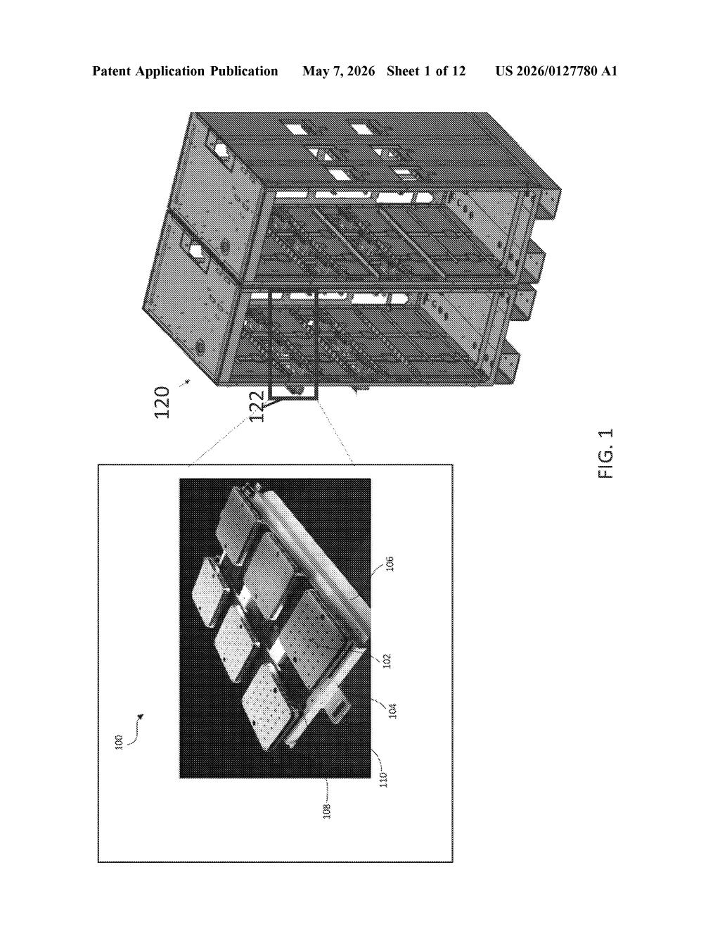
What Tesla's wafer-scale partition visualizer actually does
Imagine trying to manage a data center where instead of individual servers, your computing units are entire semiconductor wafers — each one packed with dozens of processor dies. At that scale, knowing which part of the wafer is doing what becomes a real engineering headache.
That's the problem Tesla's patent addresses. It describes a software tool that reads configuration data about a wafer-scale computing system — essentially a giant chip made from an array of wafers, each containing many dies — and generates a visual map showing how the system is divided into logical partitions and which physical dies belong to each one.
Think of it like a floor plan for a skyscraper, but for silicon. Instead of wandering hallways, engineers can look at a diagram and instantly see how the computing workload is carved up across the hardware. It's a developer and operations tool — not a consumer product — but it hints at the scale of compute Tesla is trying to wrangle.
How the system maps dies and partitions across SoW arrays
The patent describes a computing device (likely a software system or management console) that performs two core operations:
- Accessing configuration information — the system reads metadata that describes how a large computing cluster is divided into logical partitions (think isolated slices of compute, similar to how a data center might carve up virtual machines).
- Generating a graphical representation — it produces a visual diagram that maps those partitions onto the physical hardware, showing individual dies (the individual processor chips) within each partition.
The underlying hardware being visualized is an array of System on Wafers (SoWs) — a relatively exotic class of hardware where an entire silicon wafer, rather than a cut die, serves as a single computing unit. Each SoW in turn contains an array of dies bonded or integrated together. Companies like Cerebras have commercialized this approach; Tesla appears to be building its own.
The visualization tool sits above this hardware and helps engineers understand the logical-to-physical mapping — critical for debugging, resource allocation, and fault isolation in systems where a single logical job might span thousands of physical dies across multiple wafers.
What this signals about Tesla's custom silicon strategy
Wafer-scale computing is one of the more audacious bets in modern chip design. By skipping the step of cutting wafers into individual dies and packaging them separately, you can build processors with dramatically more on-chip bandwidth and fewer interconnect bottlenecks. But managing such systems requires tooling that simply doesn't exist off the shelf.
This patent suggests Tesla isn't just buying wafer-scale hardware — it's building the infrastructure software to run and manage it. That's a significant investment. For Tesla's AI training workloads (autonomous driving, robotics), having proprietary tools to manage exotic compute could be a meaningful operational advantage — and a sign that Tesla's Dojo supercomputer program is more alive than recent headlines suggested.
This is a narrow, infrastructure-level patent — not flashy on its own — but it's a meaningful data point. Tesla building custom visualization and management tooling for wafer-scale systems means they're deep enough into this architecture that off-the-shelf tools don't cut it. That's not a company dabbling; that's a company committed. Watch this space alongside any Dojo updates.
Get one Big Tech patent every Sunday
Plain English, intelligent commentary, no hype. Free.
Editorial commentary on a publicly published patent application. Not legal advice.