
Sony Patents a Three-Layer Camera Chip That Protects Itself from Electrical Damage
Sony is designing image sensors where circuit protection lives on its own dedicated silicon layer, separate from the light-capturing and signal-processing layers below it.
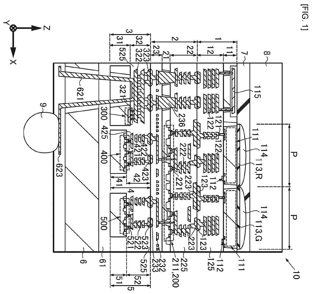
What Sony's three-chip camera sensor stack actually does
Imagine a camera sensor as a tiny factory with three departments: one team captures light, another team converts that light into a usable image, and a third team acts as the electrical safety crew. That is essentially what Sony is patenting here.
Right now, many image sensors pack all of those jobs onto one or two chips. Sony's design gives each job its own dedicated chip, stacked on top of one another. The safety layer, which absorbs unexpected electrical surges before they fry the image-processing circuitry, sits on that third chip.
The practical idea is that separating these responsibilities could let each chip be built and optimized for its specific job, without the safety circuitry crowding out the image-processing hardware or vice versa.
How Sony splits light capture, processing, and protection across three chips
The patent describes a stacked solid-state image sensor made of three distinct silicon layers (called "bases" in the filing).
- First base: Contains the photoelectric conversion elements (the photosites that turn incoming light into electrical charge, the same fundamental unit you find in every digital camera sensor).
- Second base: Contains the signal processing circuit, which reads the electrical charges from the first layer and turns them into image data.
- Third base: Contains a protection element wired to the signal processing circuit on the second base. Its job is to absorb overcurrent events, meaning sudden spikes of electrical current that could damage the delicate processing circuits above.
The key structural claim is that all three layers are physically separate chips bonded together, not regions of a single die. That separation is what the patent is specifically protecting as its novel arrangement. The protection element on the third base is electrically connected to the signal processing circuits so it can act as a shock absorber during power irregularities.
What this means for high-end camera sensors in Sony devices
Sony is one of the world's dominant image sensor suppliers, making the chips inside cameras from Apple, Google, and Sony's own devices. A stacked sensor design that dedicates an entire layer to electrical protection suggests Sony is thinking about reliability at a component level, which matters as sensors are pushed to handle faster readout speeds and higher power densities.
That said, this is a structural architecture patent, not a finished product announcement. The real question is whether the protection-on-its-own-layer approach meaningfully improves sensor longevity or yield in manufacturing compared to integrating protection circuits on the second base. That answer lives in Sony's labs, not this filing.
This is a quiet, incremental engineering patent rather than a headline-grabbing feature. Separating protection circuitry onto a third silicon layer is a logical extension of the stacked-chip trend Sony has been driving for years, and it could matter for sensor reliability in high-end cameras. But there is nothing here that signals a new product category or a dramatic capability jump.
There are more where this came from
We read every patent application Big Tech publishes and send you the ones worth knowing. Plain English, free, every week.
The drawings
22 drawing sheets from US 2026/0223473 A1 · click any drawing to enlarge


Want this weekly breakdown for a company we don't cover? Patentlyze Pro →
Be the first to weigh in