
Sony's New Patent Stacks a Camera Chip in Three Layers to Sharpen Every Shot
Sony is filing patents on a way to build image sensors from separate stacked layers, each handling a different part of the job of turning light into a photo. It's a structural approach that could shape how camera chips are designed for years.
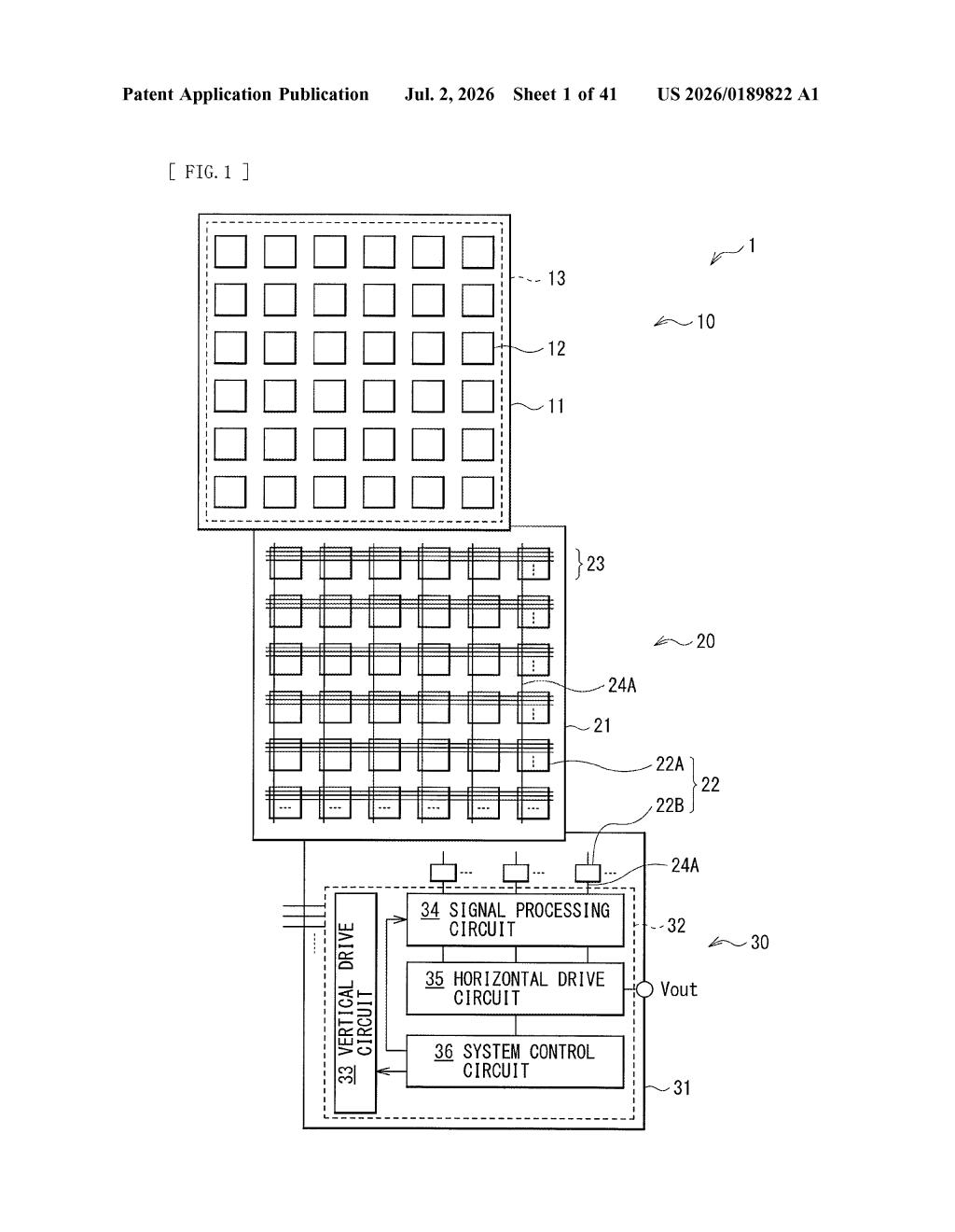
What Sony's layered image sensor chip actually does
Think of a traditional camera chip like a single employee who has to catch the light, measure it, and process the result, all at once, all in the same space. Sony's patent describes splitting those jobs across three separate chip layers stacked on top of each other, like floors in a building.
The bottom floor catches light and converts it to an electrical charge. The middle floor reads that charge and starts turning it into usable data. The top floor handles the heavy number-crunching to produce your final image. Each layer specializes in one thing.
The big idea is that separating these tasks gives engineers more freedom to optimize each layer independently. You could use the best material for light capture on one layer, and the fastest transistors for processing on another, without having to compromise between them.
How Sony splits light capture and signal processing across substrates
The patent describes a stacked image sensor built from three distinct substrates (chip layers) bonded together vertically.
- First substrate (top): Contains photoelectric conversion portions, the parts of the sensor that absorb incoming photons and turn them into electrical charge. It also houses a floating diffusion, a tiny node that temporarily holds that charge before it's read out.
- Second substrate (middle): Contains part of a readout circuit, including an amplification transistor whose gate electrode is wired directly to the floating diffusion. This transistor takes the small accumulated charge and boosts it into a measurable signal. The second substrate also holds part of a comparison circuit, which is used to evaluate and digitize that signal.
- Third substrate (bottom): Houses a logic circuit that performs image processing on the final pixel signal.
By splitting the amplification and comparison steps onto a dedicated middle layer, Sony's design avoids cramming every circuit element into the light-sensitive top layer. This matters because transistors and light-capture structures compete for space, and they each prefer different manufacturing processes.
What this means for future Sony cameras and smartphones
Stacked sensor designs have been a major battleground in camera chip engineering for the past decade, with Sony already shipping commercially. This patent suggests Sony is continuing to refine how precisely it partitions functions across layers, particularly by placing the amplification transistor and part of the comparison circuit together on a dedicated second layer.
For you as a camera user, this kind of architecture can translate to faster readout speeds (less rolling shutter distortion in video), lower noise in low light, and potentially smaller overall chip footprints. It's the kind of foundational silicon work that doesn't make headlines at a product launch but shapes what those products can actually do.
This is a fairly deep piece of semiconductor plumbing, not a flashy feature patent. But Sony Semiconductor Solutions is the image sensor supplier for a huge portion of the smartphone industry, including Apple's iPhone cameras, so even incremental refinements to their stacking architecture carry real downstream weight. Worth watching as a signal of where Sony's sensor roadmap is headed.
Get our take in your Top Stories
Liked this breakdown? Add Patentlyze as a preferred source on Google, and our plain-English take shows up more often in your Top Stories the next time Sony patent news breaks.
There are more where this came from
We read every patent application Big Tech publishes and send you the ones worth knowing. Plain English, free, every week.
Want this weekly breakdown for a company we don't cover? Patentlyze Pro →