Samsung Patents a Display That Changes How It Scans Its Own Pixels to Cut Power
Samsung is patenting a display controller that can detect a specific pixel pattern on screen and automatically switch between two different ways of refreshing the display, a move aimed at managing how much current hits individual pixels.
What Samsung's scanning-mode switch actually does
Picture a digital photo where every other row of pixels is very bright and the rows in between are nearly black. That kind of alternating pattern is common in certain UI elements, gradients, and video content. Without any special handling, your screen refreshes every row the same way, sending the same kind of electrical signal to bright and dark pixels alike.
What Samsung is patenting here is a display controller that notices when that bright-dark-bright-dark pattern exists in a frame and switches to a different refresh technique called interlaced scanning. Instead of scanning every row in order, it skips around, refreshing odd rows first and even rows next, so it can deliver current in a more controlled waveform.
The goal is to keep the electrical signal to those high-brightness rows from spiking in a way that could cause uneven wear, color shift, or power waste. It's a fairly targeted fix for a specific display-stress scenario.
How the processor detects alternating bright and dark rows
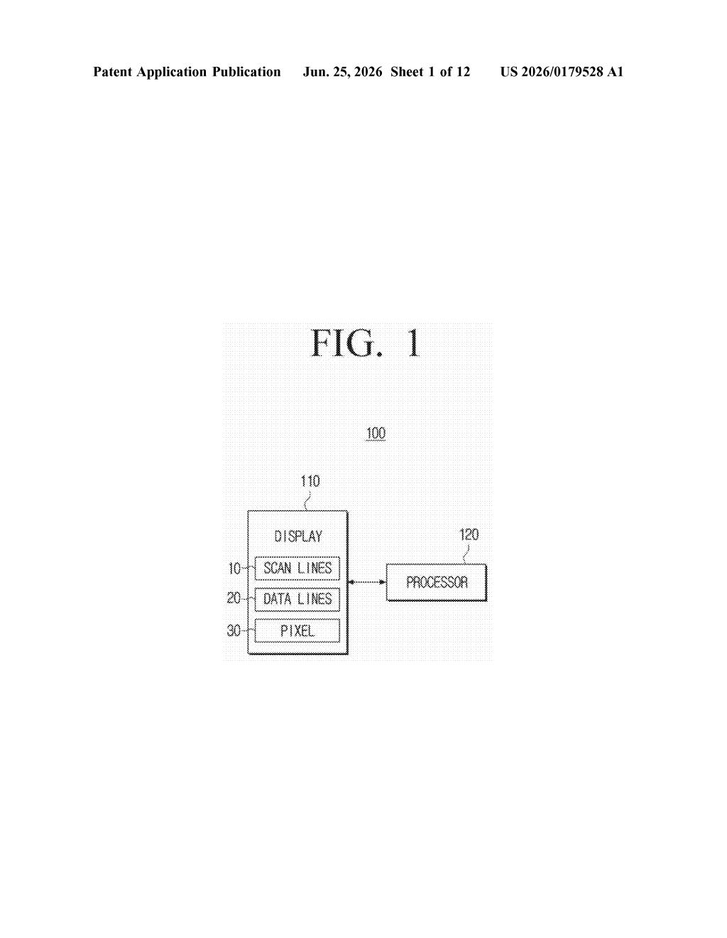
The patent describes an electronic device with a display built from intersecting scan lines (horizontal) and data lines (vertical), with pixels sitting at each intersection. This is standard display architecture.
The interesting part is how the one or more processors decide which scanning method to use for a given frame. By default, they use progressive scanning (scanning every row in sequence, top to bottom, the way modern screens typically work). But the processor continuously checks whether the incoming image frame contains an alternating pattern: a high-luminance row followed by a low-luminance row, repeating throughout the frame.
If that alternating pattern is detected, the processor switches to interlaced scanning (a technique where odd-numbered rows are refreshed in one pass and even-numbered rows in a second pass, historically used in broadcast TV). In this context, the switch isn't about video compatibility; it's about controlling the current waveform delivered to the display panel, keeping peak current more predictable when bright and dark lines sit next to each other.
The patent doesn't specify a particular display technology, but the concern about luminance-driven current spikes is most relevant to OLED and AMOLED panels, where each pixel draws current proportional to its brightness.
Why it matters
On OLED screens, bright pixels draw significantly more current than dark ones. When a frame has alternating bright and dark rows, the scan controller has to rapidly switch between high-current and low-current demands, which can stress the panel and contribute to uneven aging over time. Samsung's approach lets the hardware adapt its refresh strategy to the content, rather than treating every frame identically.
For you as a user, the practical upside would be a screen that manages pixel wear more carefully in specific content scenarios, potentially extending display lifespan or reducing the power consumed during those moments. Samsung ships OLED panels in everything from Galaxy phones to high-end televisions, so a technique like this could appear across a wide product range.
This is a narrow but sensible engineering patent. Interlaced scanning as a power and wear management tool on modern OLED displays is a clever repurposing of an old technique, and the conditional logic (only switch when the alternating pattern exists) keeps it from degrading image quality in normal use. It's not flashy, but display longevity is a real consumer pain point, especially on expensive OLED phones.
Get one Big Tech patent every Sunday
Plain English, intelligent commentary, no hype. Free.
Editorial commentary on a publicly published patent application. Not legal advice.