Samsung Patents an Image Sensor With Different-Height Walls Between Pixels
The tiny walls between pixels on a camera sensor are usually the same height everywhere. Samsung's new patent argues they shouldn't be.
What Samsung's variable pixel grid actually does
Think of a camera sensor as a grid of tiny buckets, each one catching a different color of light. Between those buckets are walls that stop light from spilling into the wrong one. Right now, those walls are typically the same height everywhere on the sensor chip.
Samsung's patent describes a sensor where the walls in the center of the chip are a different height from the walls closer to the edges. The idea is that light hits the center pixels straight-on, but hits edge pixels at an angle, so the walls need to be tuned differently in each zone to manage that light correctly.
For you as a phone owner, this kind of engineering is about getting cleaner, more accurate colors all the way to the corners of a photo, especially in low light or when shooting with a wide-angle lens where edge distortion is more noticeable.
How the stacked grid layers vary across the sensor
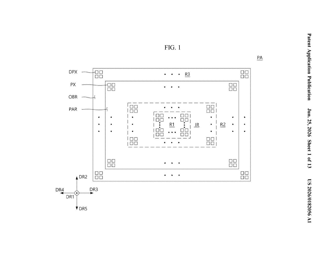
The patent describes a back-side illuminated (BSI) image sensor, meaning light enters from the back of the silicon chip rather than having to pass through the wiring layer first. That design is already standard in modern smartphone cameras.
On top of the chip's color filters sit grids, physical dividers that sit between individual pixels to prevent crosstalk (light bleeding from one pixel into a neighbor). What Samsung is patenting is a sensor divided into at least two zones:
- A first region at the center of the sensor, whose grid is made of N stacked layers
- A second region between the center and the optically blacked-out border, whose grid is made of M stacked layers
Because N and M are different integers, the grids in those two zones have different heights. The optical intuition is straightforward: off-axis light (light arriving at an angle toward the sensor edges) needs a different barrier geometry than the straight-on light hitting the center. By tailoring grid height per zone, Samsung aims to reduce color mixing and improve sensitivity across the full sensor area.
What this means for Galaxy camera image quality
Camera sensors in flagship phones are already physically very small, so squeezing out optical performance is mostly a materials and geometry problem at this point. A zoned grid approach lets Samsung tune each region of the sensor for the light angles it actually receives, rather than accepting a one-size-fits-all compromise. That matters most in wide-angle cameras, where the angle of incoming light across the sensor varies dramatically.
For Galaxy phones and Samsung's camera supply chain (Samsung makes sensors used in many Android devices beyond its own), this kind of incremental sensor refinement is exactly where competitive gains happen. It won't produce a headline-grabbing megapixel jump, but it could contribute to better edge sharpness and color accuracy in the cameras that ship in your next phone.
This is the kind of deep chip-level patent that rarely makes news but shows up in the next sensor generation. It's not a flashy invention, but zoned grid geometry is a real and practical approach to a real optical problem. Worth a note for anyone tracking Samsung's camera sensor roadmap.
Get one Big Tech patent every Sunday
Plain English, intelligent commentary, no hype. Free.
Editorial commentary on a publicly published patent application. Not legal advice.