
Samsung Patents a Camera Design That Captures More Detail in Low Light
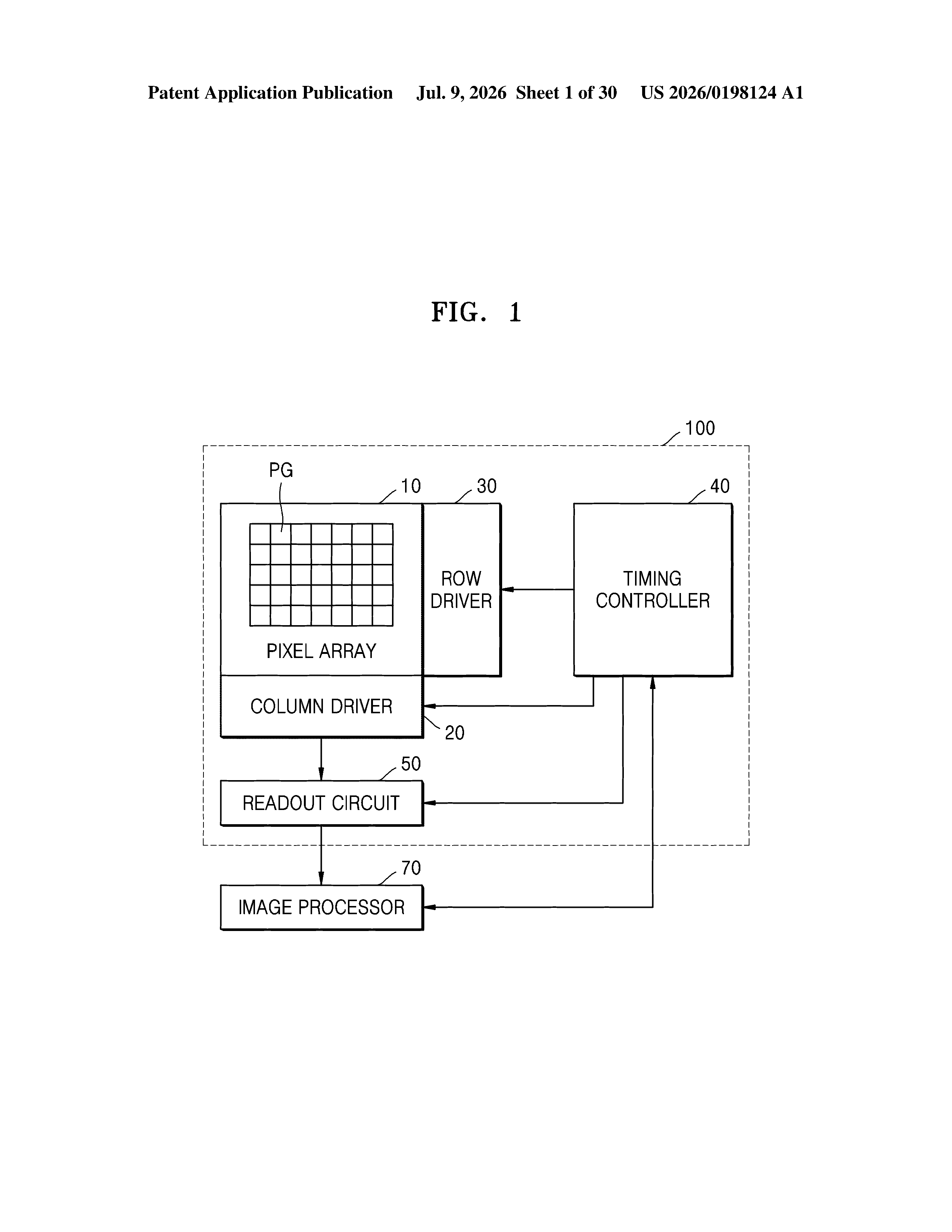
Samsung has filed a patent for a specific internal arrangement of image sensor pixels, detailing how four tiny sub-pixels are grouped, separated, and wired together to capture light more efficiently.
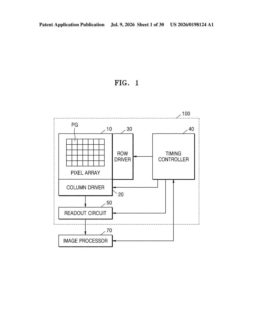
What Samsung's four-sub-pixel camera design actually does
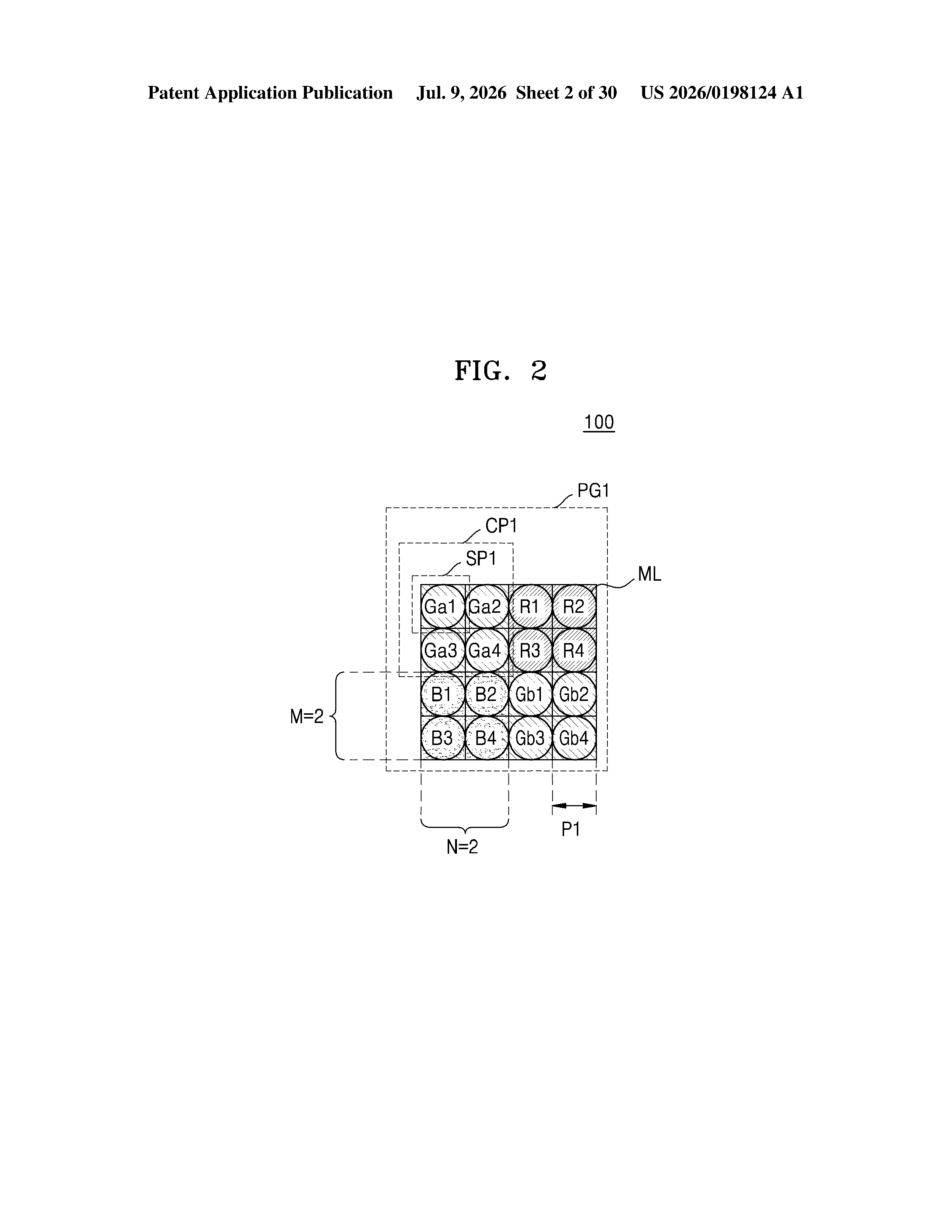
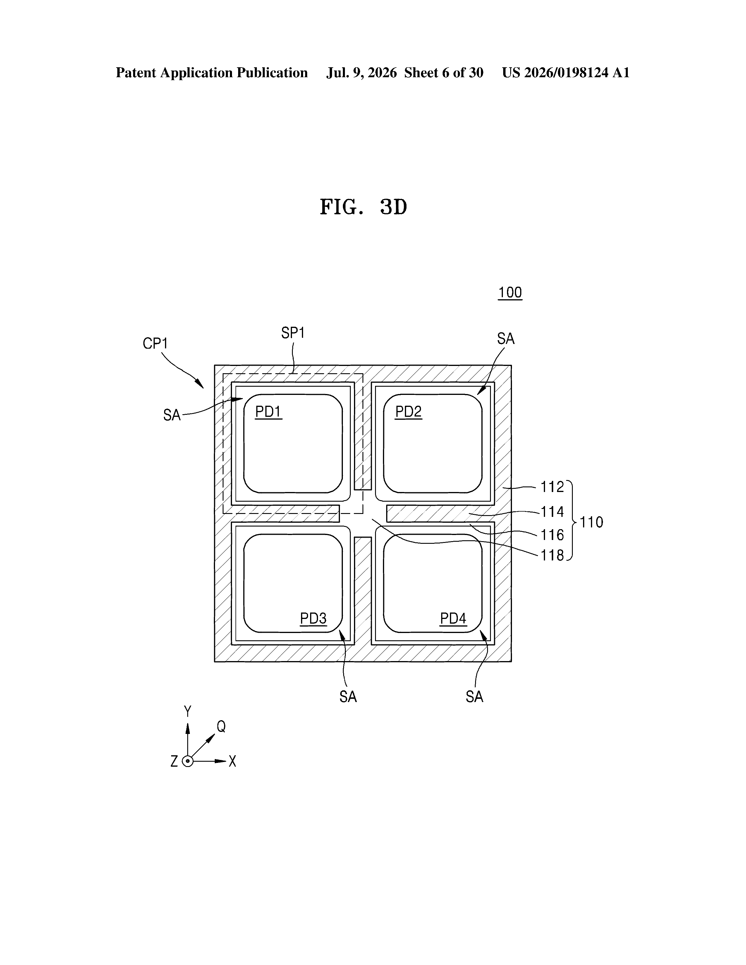
Think of a camera sensor like a mosaic made of millions of tiny tiles. Each tile captures a dot of light, and the more tiles you have, the sharper the photo. Samsung's patent describes a way to organize those tiles into groups of four, called a "unit pixel," arranged in a small 2-by-2 square.
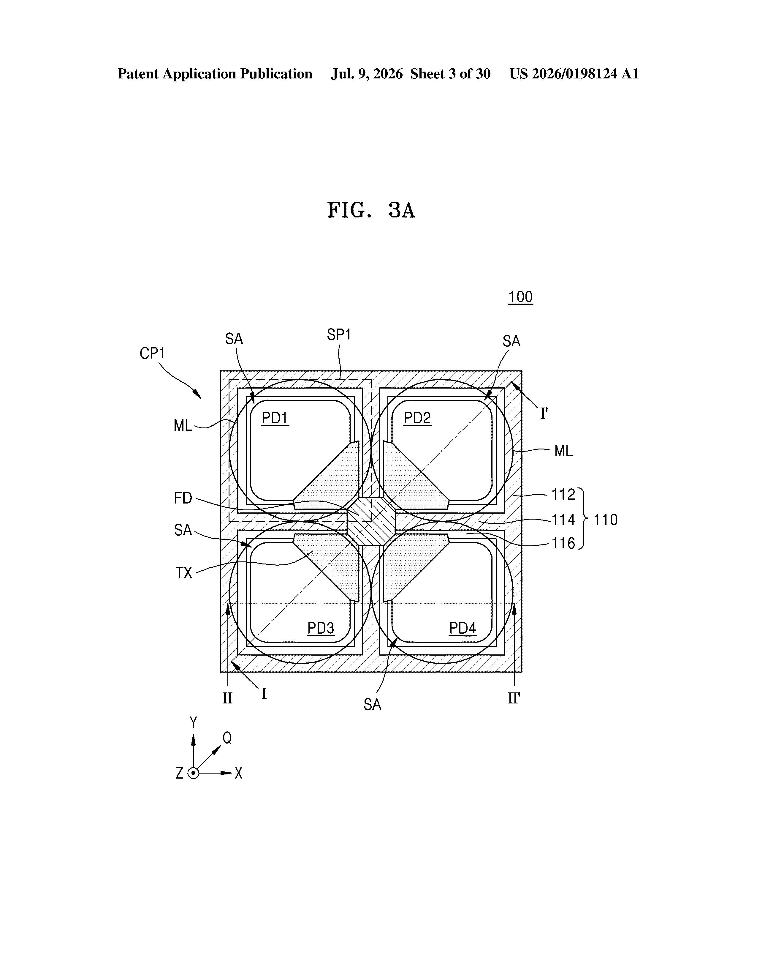
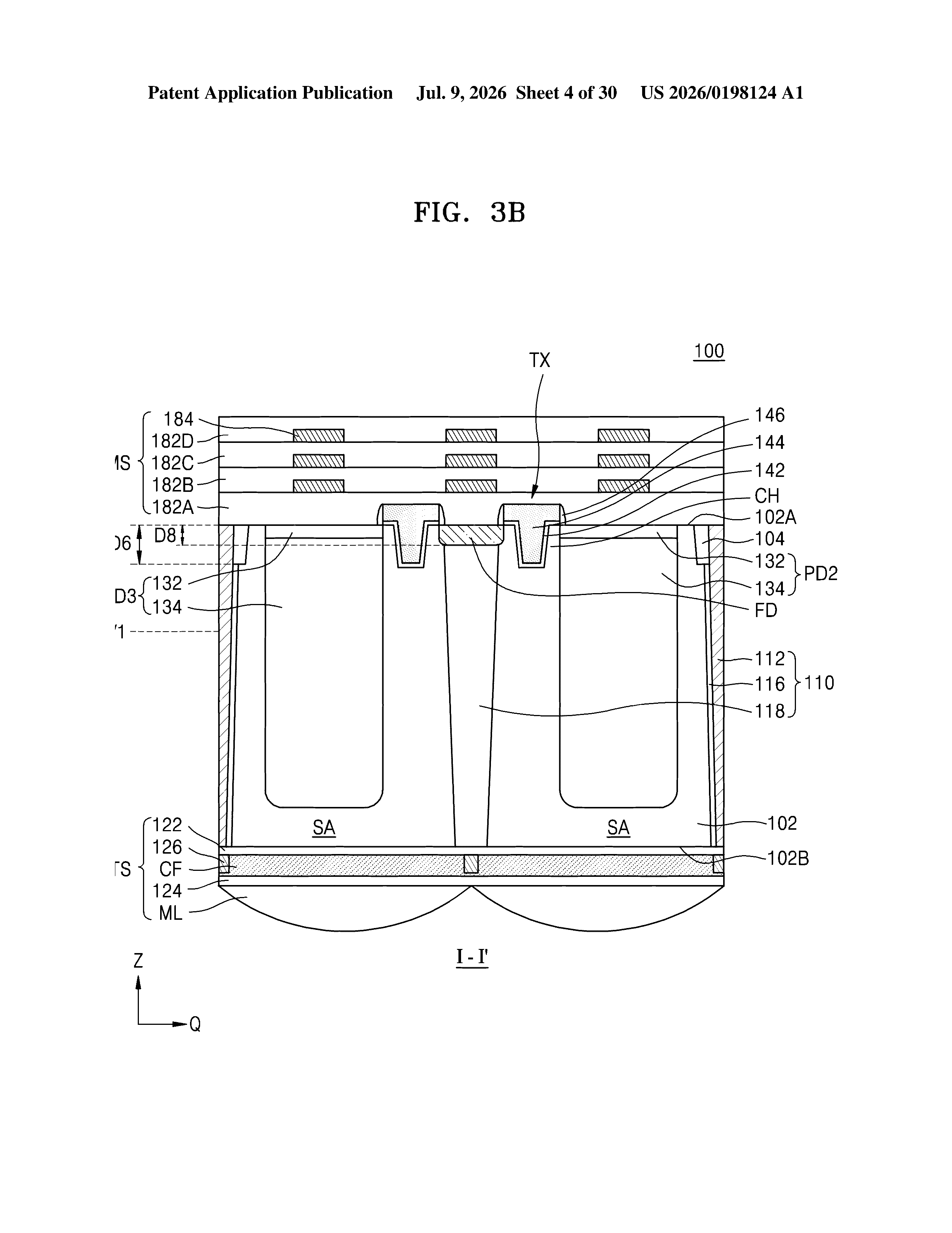
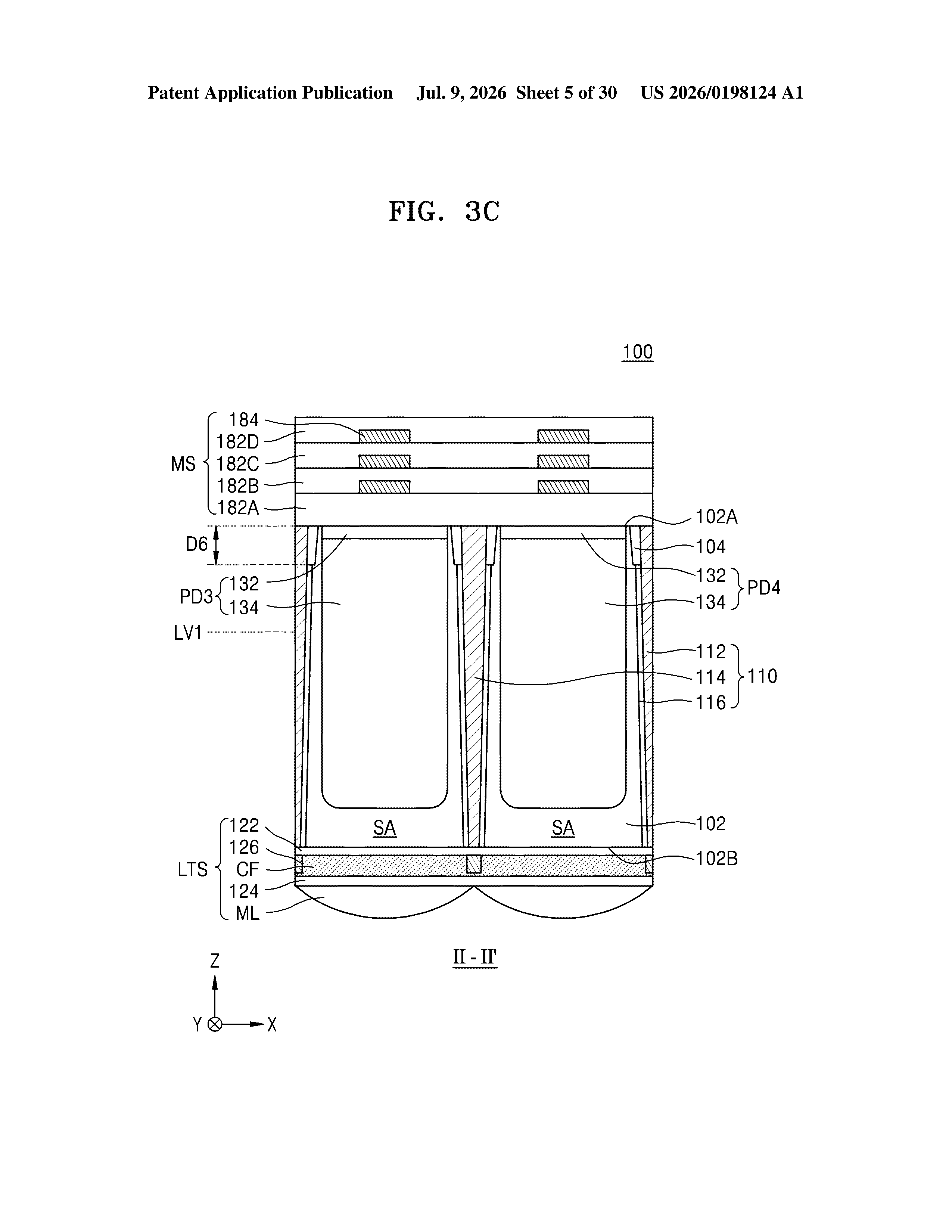
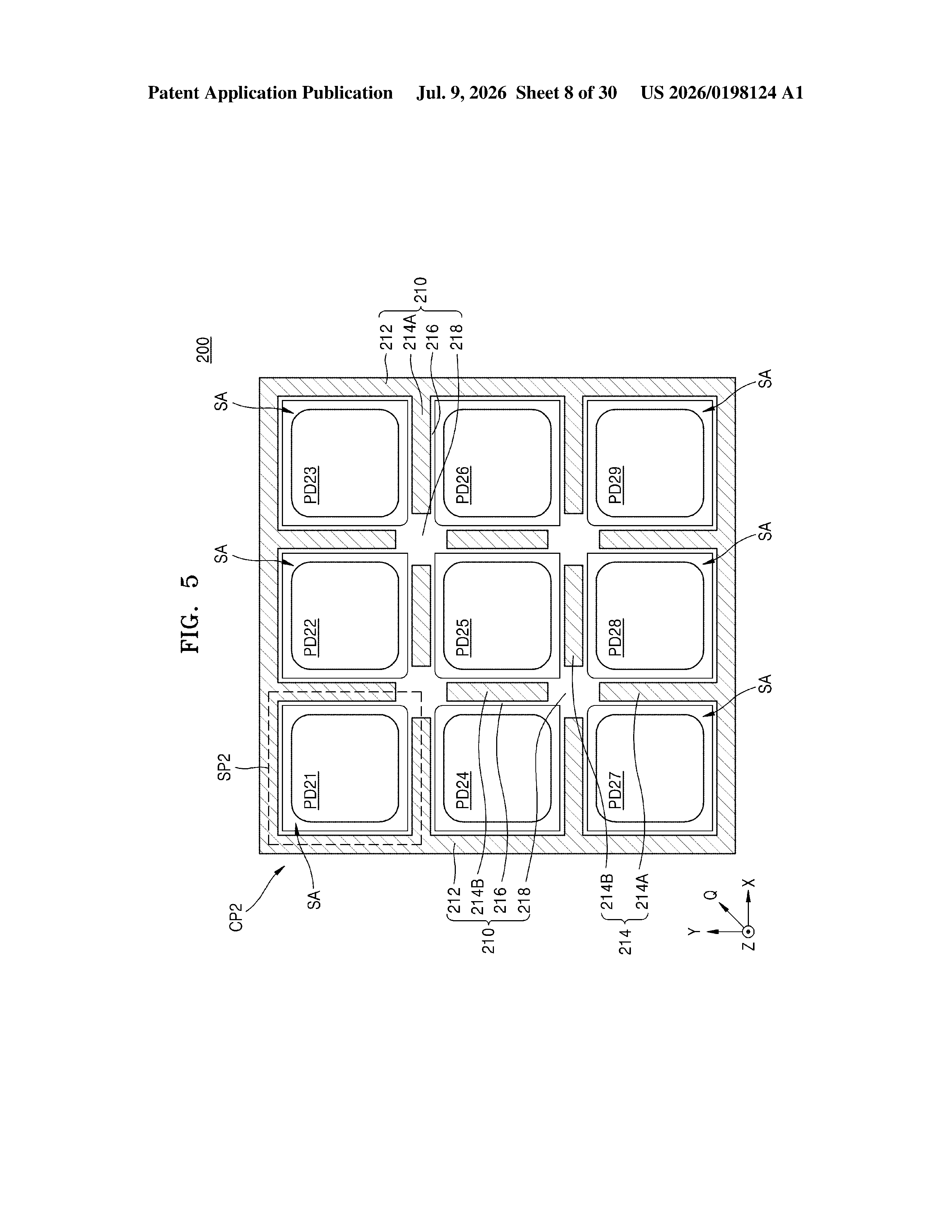
Around each group, Samsung proposes placing physical walls, called isolation trenches, to keep the groups from interfering with each other. Then, within each group, additional smaller walls separate the four individual sub-pixels. All four sub-pixels inside a group share a single electrical collection point at the center, where captured light gets converted into a signal.
The key detail is that the inner walls between sub-pixels don't all run in the same direction, which is a deliberate structural choice to reduce electrical crosstalk, the phenomenon where one sub-pixel's signal bleeds into its neighbor's. The result is cleaner light capture, especially in low-light conditions.
How the isolation trenches separate and group sub-pixels
The patent describes an image sensor architecture built around a first unit pixel, which is a cluster of four sub-pixels arranged in a clockwise 2x2 grid.
Two types of physical barriers define the structure:
- First pixel isolation trench: A continuous wall that encircles the entire four-pixel group, keeping it electrically isolated from neighboring groups.
- Second pixel isolation trench: Four internal wall segments that separate each sub-pixel from its neighbors within the group. Crucially, opposite wall segments are offset, meaning the wall between sub-pixels 1 and 2 does not line up directly with the wall between sub-pixels 3 and 4. This staggered geometry helps reduce the electrical interference (crosstalk) that causes color fringing and noise.
At the center of the group sits a floating diffusion region, a shared electrical node where all four sub-pixels deliver their captured charge. This shared-node design is common in modern high-resolution mobile sensors because it lets the sensor combine signals from all four sub-pixels in dim light or read them individually in bright light for detail.
The outer trench is lined with an isolation liner and filled with multiple inner isolation films, which fine-tune the electrical and optical properties of the barrier.
What this means for Samsung camera sensors in phones
Samsung supplies image sensors to a huge share of the global smartphone market, including its own Galaxy devices and cameras for other phone makers. This kind of pixel-isolation patent is the structural plumbing that determines how much noise, color accuracy, and low-light sensitivity a sensor can deliver. Getting these physical geometries right is what separates an acceptable camera from a great one.
For you as a phone buyer, improvements in pixel isolation translate directly to sharper photos in dark rooms and more accurate colors when shooting through glass or artificial light. This particular filing focuses on the physical layout of the sensor chip itself, which means any gains would apply at the hardware level, before any software processing even starts.
This is a semiconductor process patent, detailed and specific, but not a flashy product announcement. It is the kind of foundational engineering work that determines whether next year's Galaxy camera beats the competition. If you follow mobile photography hardware, it is worth tracking. If you don't, there is nothing here that changes your day.
Get our take in your Top Stories
Liked this breakdown? Add Patentlyze as a preferred source on Google, and our plain-English take shows up more often in your Top Stories the next time Samsung patent news breaks.
There are more where this came from
We read every patent application Big Tech publishes and send you the ones worth knowing. Plain English, free, every week.
The drawings
30 drawing sheets from US 2026/0198124 A1 · click any drawing to enlarge
Want this weekly breakdown for a company we don't cover? Patentlyze Pro →