
Samsung Patents an Image Sensor That Focuses Light With Nano-Scale Pillars
Instead of the tiny curved glass lenses that have focused light in camera sensors for decades, Samsung is experimenting with forests of microscopic pillars to do the same job, potentially with more precision and in a thinner package.
What Samsung's nano-pillar camera sensor actually does
Imagine the world's smallest magnifying glass. Every pixel in your phone's camera sensor has one of these tiny lenses sitting on top of it, bending incoming light down onto the light-detecting surface below. Right now those lenses are curved bumps, and making them perfectly uniform at that scale is genuinely hard.
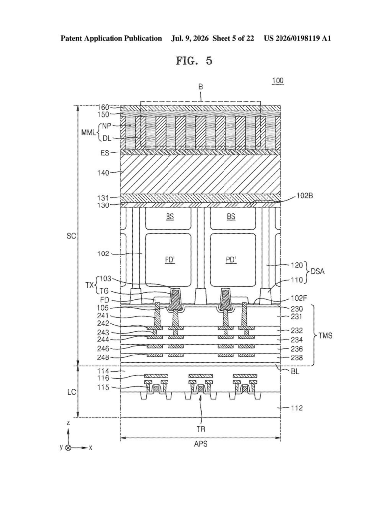
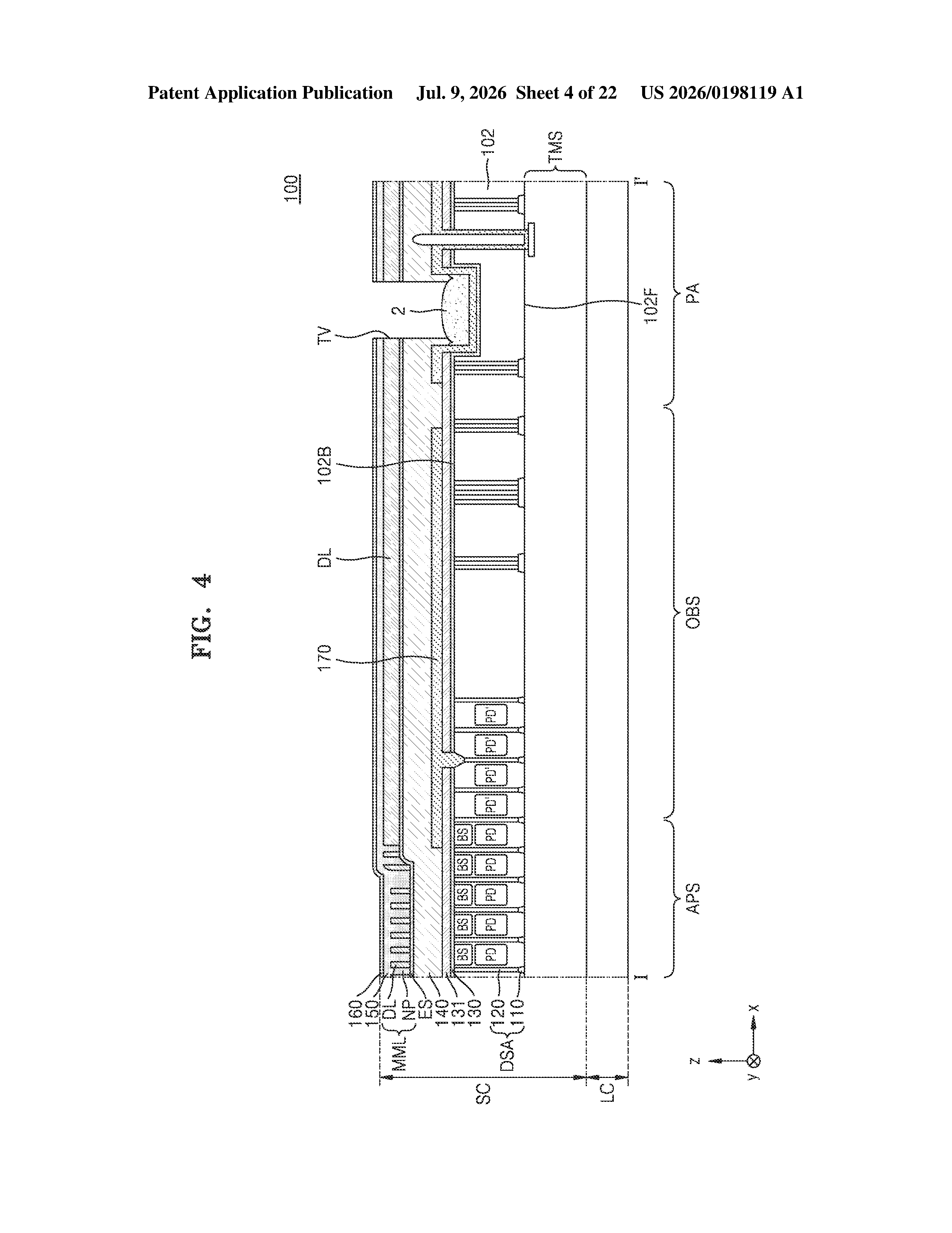
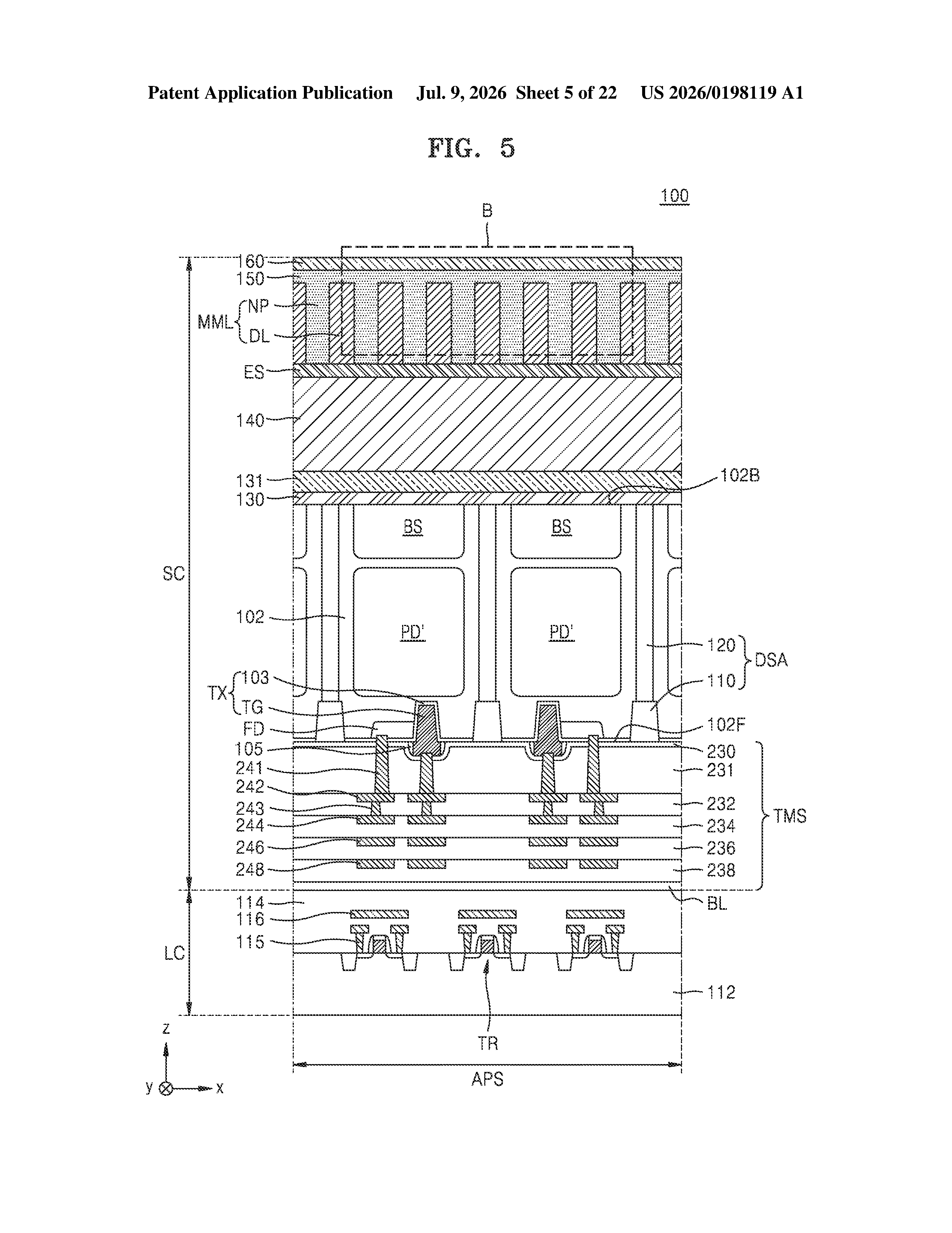
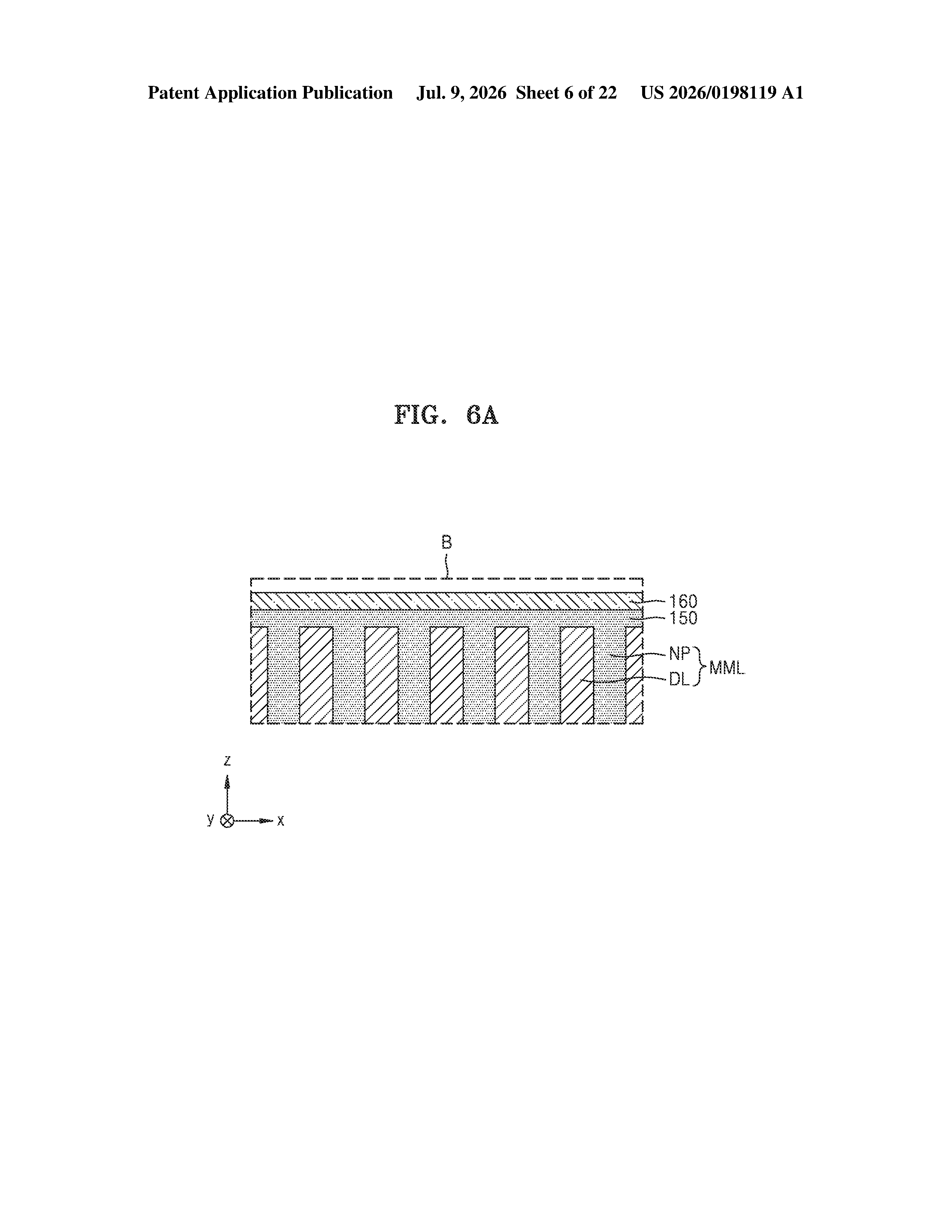
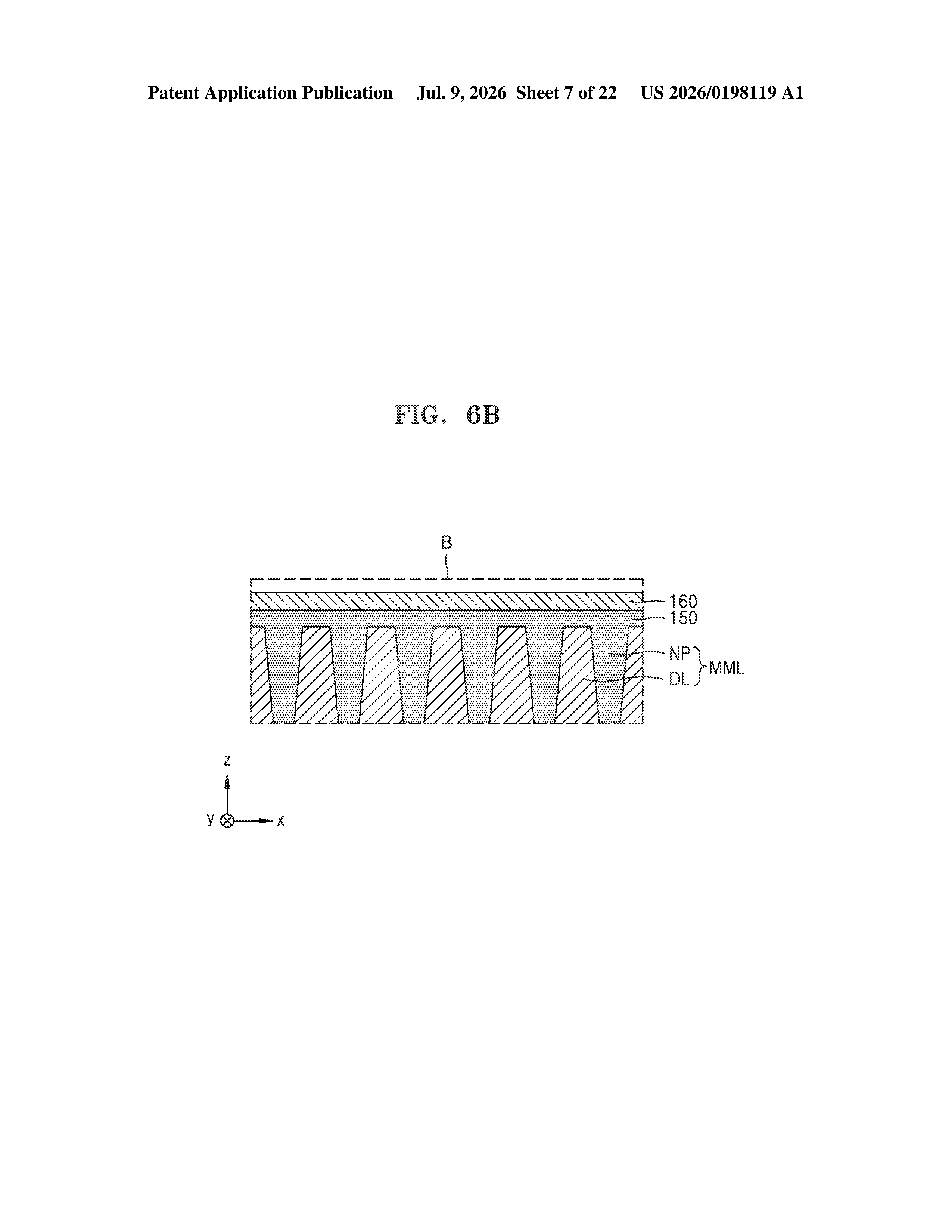
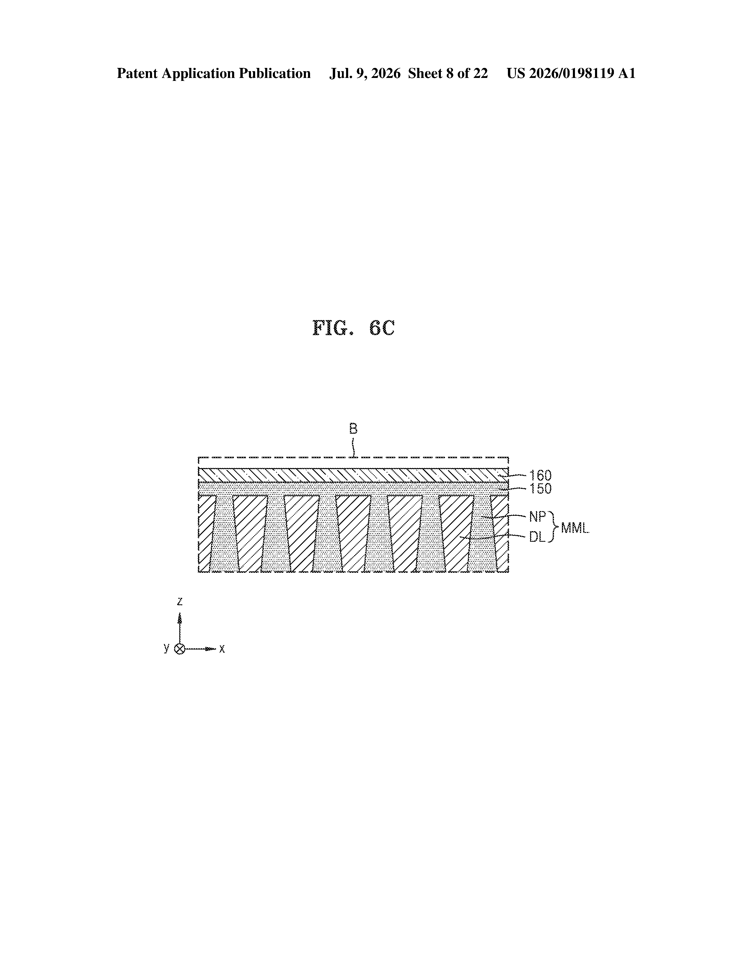
Samsung's patent describes replacing those curved bumps with a meta microlens: a flat layer of material studded with countless upright nano-scale pillars (called nano-posts) that bend light by changing how it interacts with the pillars' shape and spacing, not their physical curve. On top of that, a thin anti-reflection coating is bonded to the tops of the pillars through a connecting layer, keeping the whole sandwich firmly together.
The result is a flatter, potentially more precise lens structure that sits right on the image sensor chip itself. Whether you'd notice the difference in your photos depends on how well it translates from the lab, but it's the kind of foundational hardware work that improves low-light performance and sharpness over time.
How the meta microlens stack bends and captures light
A conventional image sensor pixel has a tiny dome-shaped microlens on top that concentrates light onto the photodetector below. Samsung's patent replaces that dome with a meta microlens, a flat structure built from two main parts:
- Dielectric layer: A flat, transparent base material that sits over the pixel.
- Nano-posts: Tiny vertical pillars (far smaller than a human hair) that poke up through the dielectric layer. By varying the height, width, and spacing of these pillars, engineers can control exactly how light bends as it passes through, mimicking what a curved lens does but in a flat form factor.
On top of that meta microlens sits a reflection prevention layer (an anti-reflection coating that stops light from bouncing off the surface rather than passing through). The key engineering detail in this patent is a nano-post connection layer that bonds the tops of the pillars directly to that anti-reflection coating. This physical contact is important: without it, the two layers could separate or trap air gaps that degrade optical performance.
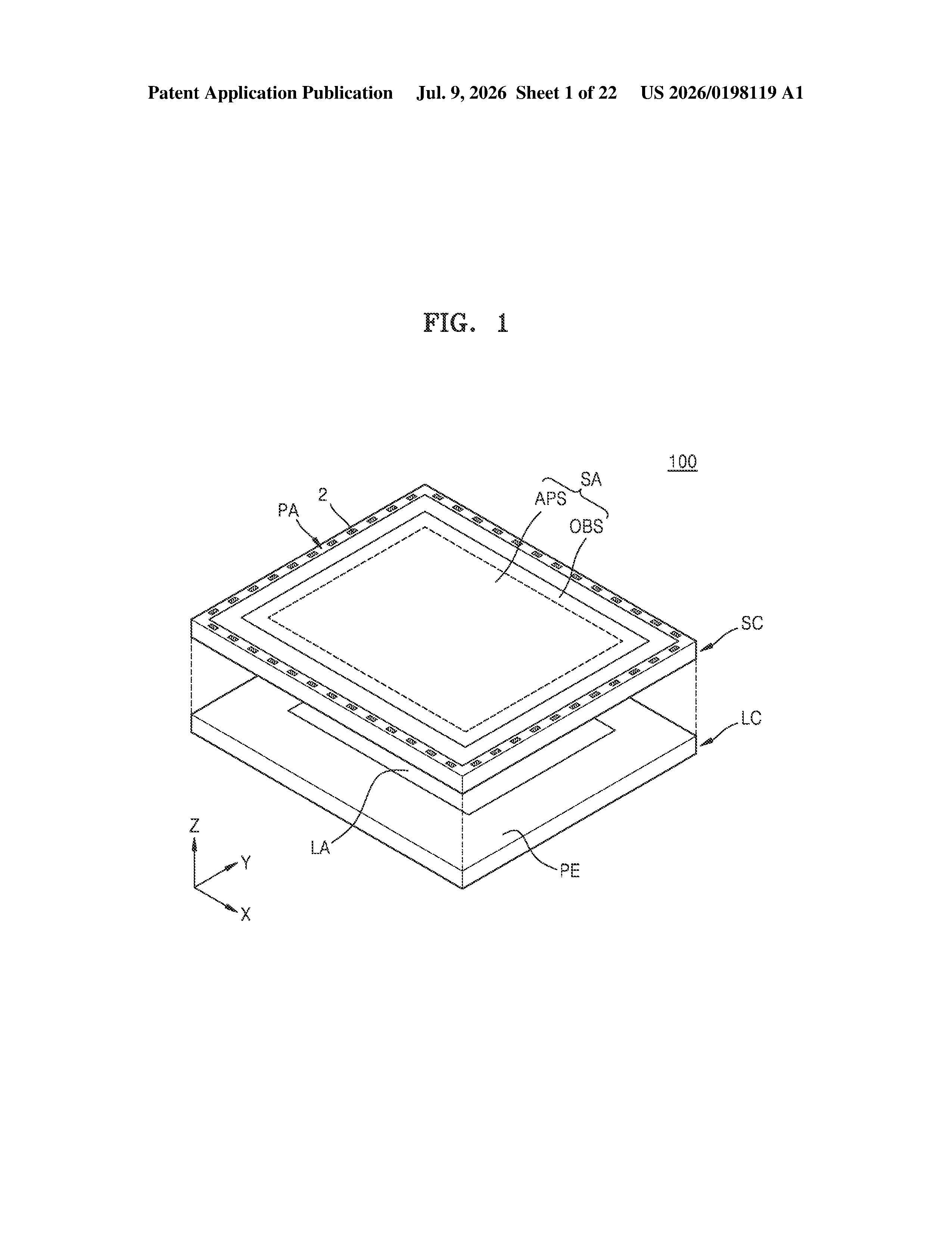
The architecture is essentially a precisely engineered optical sandwich, all built at the chip fabrication level rather than added as a separate component afterward.
What this means for future Samsung camera hardware
Meta lenses are an active area of research across the semiconductor industry because they promise thinner, lighter optical systems that are easier to manufacture consistently at scale. For Samsung, which makes image sensors for its own Galaxy phones as well as supplying other manufacturers, any improvement in per-pixel light collection translates directly into better low-light photos and sharper images at a given sensor size.
The specific bonding detail (the connection layer touching the tops of the nano-posts) suggests Samsung's engineers ran into delamination or air-gap problems in earlier designs and this is their fix. That kind of incremental structural improvement is exactly what separates a working prototype from something you can actually build millions of times in a factory.
This is deep, unglamorous fab-process work, and it probably won't show up in a press release. But image sensor architecture is where phone camera quality actually gets made, and Samsung is one of the few companies with both the sensor-design and chip-manufacturing capabilities to turn a meta-lens concept into a shipping product. Worth tracking if you follow mobile camera hardware.
Get our take in your Top Stories
Liked this breakdown? Add Patentlyze as a preferred source on Google, and our plain-English take shows up more often in your Top Stories the next time Samsung patent news breaks.
There are more where this came from
We read every patent application Big Tech publishes and send you the ones worth knowing. Plain English, free, every week.
The drawings
22 drawing sheets from US 2026/0198119 A1 · click any drawing to enlarge
Want this weekly breakdown for a company we don't cover? Patentlyze Pro →