
Samsung Patents a New Way to Wire Pixels Together Inside a Camera Chip
Samsung is rethinking how individual pixels inside a camera sensor talk to each other, using a shared metal pad that bridges two pixels at the substrate level instead of relying on separate wiring for each one.
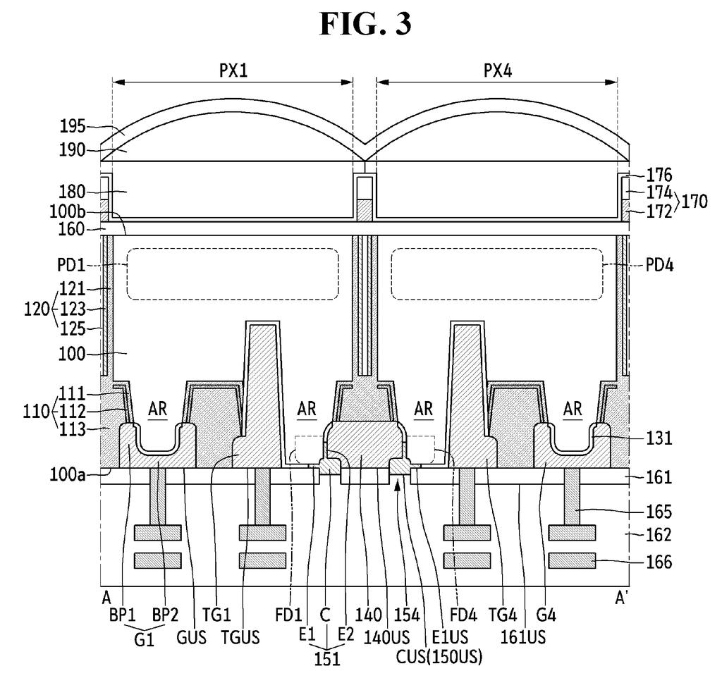
How Samsung's shared pixel pad changes camera chip wiring
Imagine a camera chip as a grid of millions of tiny light-collecting buckets, each one reporting back how much light it caught. Right now, each bucket needs its own dedicated wiring path to send that signal out. Samsung's patent describes a smarter physical arrangement where two neighboring buckets share a single connector between them, built right into the chip's base layer.
The key piece is a small metal bridge called a connection pad, sitting between two pixels and physically touching both of them through a set of extension arms. Those arms reach along the surface and down into the chip material itself, giving the connection a larger contact area and a more stable grip.
For everyday users, this kind of internal architecture tweak is invisible, but it's exactly the sort of low-level engineering that affects how cleanly a sensor reads light, especially in low-light conditions where every bit of signal matters.
How the extension pads and connection pad fit together
The patent describes an image sensor built on a substrate (the base chip material) that contains two neighboring pixels. Each pixel has a floating diffusion region, which is the tiny area that collects the electrical charge generated when light hits the sensor and converts it into a voltage signal that the camera's processor can read.
Instead of wiring each floating diffusion region independently, Samsung's design introduces a connection pad that sits physically between the two pixels and contacts both of them at once. Each pixel gets its own intermediate pad structure with three parts:
- An extension portion that runs along the surface of the floating diffusion region and makes direct contact with it
- A second extension portion that dips down into the substrate material below
- A connection portion that joins those two arms together
The shared connection pad then bridges the two pixel-side pads, creating a linked electrical path. The multi-arm shape gives each contact point a larger physical footprint inside the chip, which can reduce electrical resistance and improve how reliably the charge signal transfers.
What this means for future Samsung camera sensors
Camera sensor engineering at this physical level directly affects image quality metrics like read noise (the electronic static that masks fine detail) and charge transfer efficiency (how completely the light signal moves from the collection point to the readout circuit). A more reliable connection between the floating diffusion region and its output path means cleaner data before any software processing even starts.
Samsung is one of the world's largest image sensor manufacturers, supplying chips for its own Galaxy phones and for many other device makers. Patents like this one reflect the incremental, highly competitive work happening at the transistor-and-metal level of sensor design, where fractions of a decibel in noise performance can separate one generation of camera hardware from the next.
This is deep-in-the-stack semiconductor engineering with no flashy product story attached. The patent covers a specific physical pad geometry, not a new camera feature users would ever see named on a spec sheet. That said, floating diffusion design is a genuine battleground in image sensor competition, and Samsung filing here signals continued investment in the foundational physics of image capture.
There are more where this came from
We read every patent application Big Tech publishes and send you the ones worth knowing. Plain English, free, every week.
The drawings
46 drawing sheets from US 2026/0215020 A1 · click any drawing to enlarge


Want this weekly breakdown for a company we don't cover? Patentlyze Pro →
Be the first to weigh in