
Samsung Patents an Image Sensor That Uses Atom-Thin Materials to Separate Pixels
Samsung is filing patents on a way to build tighter walls between camera pixels using materials that are just a few atoms thick, which could help sensors capture more accurate color and detail, especially in low light.
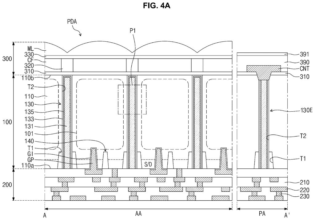
What Samsung's atom-thin pixel barrier actually does
Imagine a camera sensor as a grid of tiny buckets, each designed to catch light and report a color. The problem is that light landing in one bucket can "slosh" into neighboring buckets, causing colors to bleed together and fine details to blur. This is a real challenge as phone cameras cram more and more pixels into a smaller and smaller space.
Samsung's patent describes a new kind of divider wall placed between each pixel. Instead of simple barriers, these walls are built from layers that include so-called two-dimensional materials, meaning substances (like graphene) whose useful structure exists in sheets that are just one or a few atoms thick. That thinness matters: thinner walls mean more room for each light-catching pixel.
The design stacks an insulating layer (to block electricity from leaking between pixels) and a conductive layer (to help drain away stray electric charge) inside a narrow trench cut into the silicon. Using 2D materials for these layers means the walls can be made very precisely without taking up the space that thicker conventional materials would require.
How the layered isolation trench keeps pixels from bleeding
The patent covers an image sensor built on a semiconductor substrate (a slice of silicon) with photodiodes, tiny light-detecting elements, etched into it. Between each photodiode is a narrow trench called a PD isolation pattern (PD stands for photodiode), which acts as the dividing wall.
Inside that trench, Samsung stacks three distinct layers:
- Insulating pattern: the core fill of the trench, blocking electrical signals from crossing between pixels.
- Insulating liner: a thin layer between the core and the silicon, preventing charge from leaking at the interface.
- Conductive liner: a thin electrically active layer sandwiched between the other two, used to apply a bias voltage (a controlled electrical field) that sweeps stray electrons away from the pixel boundary.
The key innovation is that at least one of those liner layers is made from a two-dimensional material, a category that includes substances like graphene and molybdenum disulfide whose crystal structure forms a flat sheet only one or a few atoms thick. Depositing these materials uniformly inside a very narrow trench is technically difficult but allows the total wall thickness to stay extremely small, which becomes critical when pixels are already measured in fractions of a micrometer.
What this means for Samsung camera sensor quality
As smartphone cameras push toward higher pixel counts, each individual pixel shrinks. That makes cross-talk (light or charge from one pixel contaminating its neighbor) an increasingly serious problem and one that limits how sharp and color-accurate photos can look. Better isolation walls directly improve the signal from each pixel, which translates to cleaner images, especially in dim conditions where every captured photon counts.
Samsung's sensor division supplies image sensors not only to its own Galaxy phones but to other manufacturers. An improvement in isolation technology at this level of the fabrication process could ripple across a wide range of devices. Whether this particular design makes it into production is a separate question, but it signals that Samsung is actively working on next-generation pixel isolation at the materials level.
This is a materials-engineering patent aimed at a real and well-documented problem in miniaturized camera sensors. It's not a flashy consumer feature, but the underlying challenge (keeping shrinking pixels from interfering with each other) is genuinely hard, and using 2D materials to solve it is a credible approach that several research groups have been exploring. Worth tracking if you follow camera sensor development.
There are more where this came from
We read every patent application Big Tech publishes and send you the ones worth knowing. Plain English, free, every week.
The drawings
33 drawing sheets from US 2026/0215015 A1 · click any drawing to enlarge


Want this weekly breakdown for a company we don't cover? Patentlyze Pro →
Be the first to weigh in