
Samsung Patents a Camera Pixel Structure Built to Capture Sharper, Cleaner Photos
Samsung is patenting a new way to build the transistors inside individual camera sensor pixels, stacking gate layers to pack more control circuitry into a tighter space.
What Samsung's stacked pixel gate design actually does
Imagine each pixel in your phone's camera sensor as a tiny bucket that catches light. Inside that bucket is a set of tiny switches that move the captured light signal out to be processed into the photo you see on screen. The more precisely those switches work, the cleaner your photo.
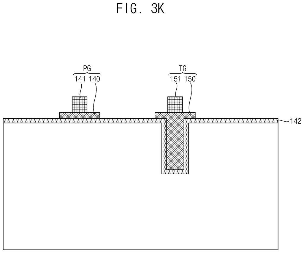
Samsung's patent describes a new way to build those switches, called gates, by layering them in two parts: a lower section and an upper section stacked on top. This applies to two key transistors inside each pixel, the one that transfers the light signal and the one that helps process it.
The practical idea is that splitting each gate into two stacked layers gives engineers finer control over how the pixel operates. That can translate into less electrical noise and better light-to-signal conversion, especially in low-light conditions where your camera tends to struggle most.
How the two-layer gate structure sits inside each pixel
Each pixel in a camera image sensor contains a photodiode (the part that absorbs incoming light and converts it to an electrical charge) and a set of transistors that move and amplify that charge so it can be read out as image data.
Samsung's patent focuses on two of those transistors. The first is the transfer gate transistor, which acts like a valve between the photodiode and a holding area called the floating diffusion region. The second is a companion transistor nearby. In both cases, the patent describes the gate (the control electrode that opens and closes the transistor) as being built in two stacked layers: a lower gate sitting directly on the semiconductor substrate and an upper gate on top of it.
The photodiode sits in the lower portion of the semiconductor substrate, while the floating diffusion region and the transistor source and drain contacts sit in the upper portion. This vertical arrangement, combined with the two-part gate structure, is the core of what Samsung is claiming.
The two-layer gate approach gives chip designers more variables to tune, including gate material, thickness, and electrical properties at each layer, which can improve how efficiently charge moves through the pixel and reduce unwanted electrical leakage.
What this means for Samsung's future camera image sensors
Image sensor performance lives and dies by what happens at the pixel level. Samsung is one of the world's largest image sensor manufacturers, supplying chips to its own Galaxy phones as well as other device makers. A patent like this signals ongoing work to refine the fundamental transistor geometry inside each pixel, which is the kind of low-level engineering that eventually shows up as improved low-light photography or reduced image noise in real products.
That said, this is a manufacturing-level structural patent, not a camera feature patent. The improvements it enables, if any make it into production chips, would be invisible to you as a user. You would just notice that photos look a bit cleaner in dim light, without knowing why.
This is a fairly narrow semiconductor fabrication patent covering a specific transistor gate geometry inside image sensor pixels. It is not the kind of filing that points to a new product or a visible feature. It is the kind of quiet, incremental engineering work that keeps Samsung competitive at the chip level, but it is not something most readers need to follow closely.
There are more where this came from
We read every patent application Big Tech publishes and send you the ones worth knowing. Plain English, free, every week.
The drawings
37 drawing sheets from US 2026/0215007 A1 · click any drawing to enlarge


Want this weekly breakdown for a company we don't cover? Patentlyze Pro →
Be the first to weigh in