
Samsung Patents a Chip-Scale LiDAR Sensor That Steers Light With Nano-Structures
LiDAR sensors, the 3D-scanning technology that helps cars and robots understand the world around them, are typically bulky and expensive. Samsung is patenting a way to shrink the whole thing down to a silicon chip.
What Samsung's miniaturized LiDAR chip actually does
Imagine a spinning laser tower on top of a self-driving car. Now imagine shrinking that entire system down to a chip the size of your fingernail and embedding it in a phone or a robot. That's the direction Samsung's latest patent is pointing.
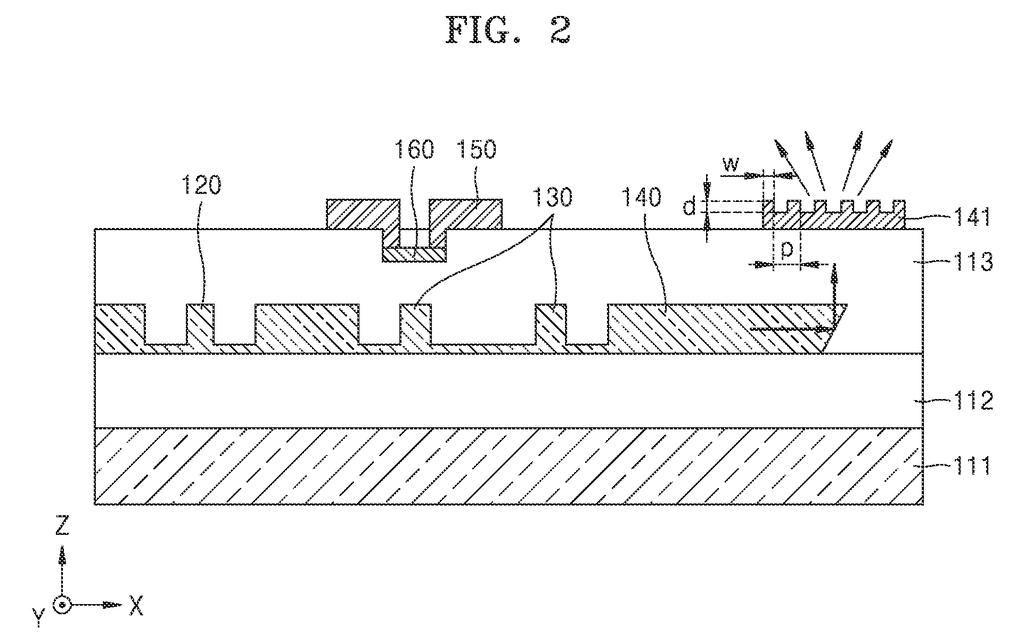
The design describes an optical sensor made up of tiny pixels on a chip. Each pixel has a small switch that controls whether light passes through it, and a specially angled surface that bends the light in a new direction before sending it out. Tiny structures, too small to see with the naked eye, then shape the beam further.
The result is a chip that can scan a scene with light pulses without any moving parts, which is how LiDAR devices traditionally work. This kind of solid-state approach could make 3D sensing far cheaper and compact enough to fit inside consumer electronics.
How light travels through Samsung's pixel-and-waveguide design
The patent describes a focal plane array (FPA), which is essentially a grid of light-sensing and light-emitting pixels all built onto the same chip substrate. Instead of a spinning mirror or mechanical actuator directing a laser beam, this system routes light through on-chip waveguides (tiny channels that guide light the way copper wires guide electricity).
Each pixel in the array contains three key components:
- An optical switch that opens or closes to let light pass through to that specific pixel, allowing the system to address pixels individually.
- An output coupler with an inclined side surface, essentially a built-in angled mirror that redirects the light beam from traveling horizontally along the chip to shooting out vertically (or at a controlled angle) into the scene.
- A nano-structure element, a surface patterned with features smaller than the wavelength of light, which acts like a lens or diffraction grating to further shape and steer the outgoing beam.
The combination of the angled coupler and the nano-structure gives the system precise control over beam direction without any moving parts. This solid-state approach is the core engineering challenge in making LiDAR practical for mass-market use.
What this means for smaller, cheaper LiDAR in consumer devices
LiDAR is already inside Apple's iPhone Pro and iPad Pro for augmented reality depth sensing, and it's a core component in autonomous vehicles and robotics. The problem is that high-resolution LiDAR capable of scanning a wide scene still relies on mechanical parts or expensive photonic components that are hard to miniaturize.
A pixel-addressable, all-on-chip design like this one could push LiDAR resolution and reliability up while pushing cost and size down. For Samsung, which supplies components to both its own Galaxy devices and third-party manufacturers, a viable solid-state LiDAR chip would fit squarely into the company's sensor business and could appear in everything from smartphones to industrial robots.
This is a serious photonics patent, not a speculative moonshot. The combination of on-chip waveguide routing, pixel-level optical switching, and nano-structure beam shaping is exactly the architecture the LiDAR industry is racing to perfect. Samsung doesn't publish many optical-chip patents like this, which makes it worth tracking.
There are more where this came from
We read every patent application Big Tech publishes and send you the ones worth knowing. Plain English, free, every week.
The drawings
20 drawing sheets from US 2026/0219367 A1 · click any drawing to enlarge


Want this weekly breakdown for a company we don't cover? Patentlyze Pro →
Be the first to weigh in