
Samsung Patents a Chip Design That Embeds Processors Directly Alongside the Memory
Moving data from memory to a processor is one of the biggest speed and power drains in modern computing. Samsung's new patent tries to eliminate much of that trip entirely by putting the compute right inside the memory package.
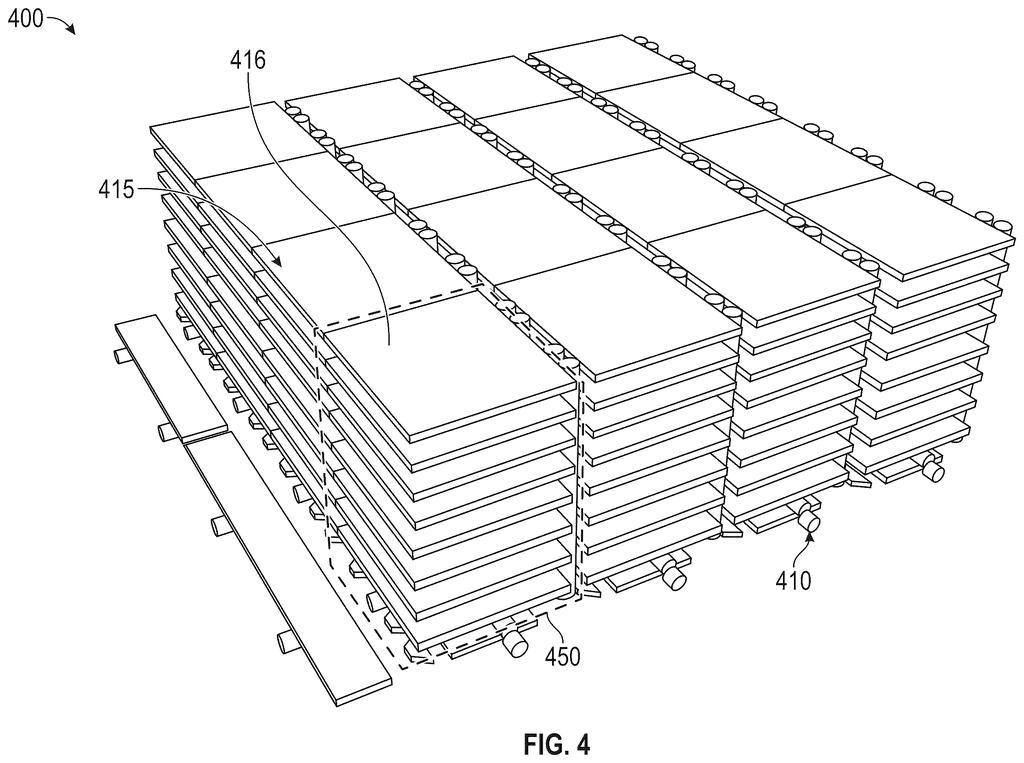
What Samsung's memory-plus-processor stack actually does
Imagine a library where every time a researcher needs a book, they have to walk across town to get it. That's roughly how most chips work today: the processor sits in one place, memory sits somewhere else, and data has to travel back and forth constantly. That trip wastes time and energy.
Samsung's patent describes a chip package where the processor cores and the memory chips are physically stacked on top of each other, connected by tiny vertical wires drilled straight through the silicon. Each processor core gets its own dedicated slice of memory right above it, so data barely has to move at all.
The design is aimed at workloads like AI inference and large-scale data crunching, where the gap between processor speed and memory access speed is the main bottleneck. By shrinking that gap to almost nothing, Samsung is betting it can build chips that are both faster and more power-efficient for those tasks.
How the TSV wiring connects each core to its own memory bank
The patent describes what Samsung calls a Compute with Memory Stack (CMS) architecture. The core idea is a multi-die package: a logic die (the layer that contains the actual processor cores) sits at the bottom, and one or more DRAM dies (memory layers) are stacked directly on top of it.
The two layers are connected by Through Silicon Vias (TSVs), which are essentially microscopic copper tubes drilled vertically through the silicon chips. TSVs are already used in high-bandwidth memory (HBM) chips, but this patent maps each set of TSVs to a specific processor core rather than sharing one big bus across everything.
- The logic die contains at least two independent compute components (processor cores or compute engines).
- Each compute component has its own dedicated set of TSVs running up through the stack.
- Each set of TSVs connects to a matching memory bank module on the DRAM die above it.
The result is a partitioned memory architecture: core one talks only to its assigned memory region, core two talks only to its own region, and so on. This avoids memory bus congestion (the traffic jam that happens when multiple processors compete to access the same memory channel at the same time).
What this means for AI chips and data-center bottlenecks
The bottleneck between processors and memory is one of the defining constraints in AI hardware right now. Large language models and matrix-heavy workloads constantly shuttle enormous amounts of data between compute and memory, and the speed of that connection often matters more than raw processor clock speed. Samsung's partitioned approach could reduce that congestion significantly by giving each core a private, high-speed memory lane.
Samsung is one of the world's largest DRAM manufacturers, and this patent signals the company is pushing deeper into the compute-in-memory space where rivals like SK Hynix (with HBM3) and Micron are also competing. If this architecture reaches production, it could show up in AI accelerators, data-center chips, or eventually consumer hardware where battery life and processing speed need to improve together.
This is a genuinely interesting structural bet on where AI chip design is heading. The idea of partitioning memory banks to private processor cores is a real architectural improvement, not just a materials tweak. Whether Samsung can manufacture this at scale and at competitive cost is the real question, but the patent shows they're thinking several steps ahead of conventional memory design.
There are more where this came from
We read every patent application Big Tech publishes and send you the ones worth knowing. Plain English, free, every week.
The drawings
10 drawing sheets from US 2026/0219786 A1 · click any drawing to enlarge


Want this weekly breakdown for a company we don't cover? Patentlyze Pro →