Samsung Patents a Stacked Nanosheet Transistor Design with Built-In PN Junction
Samsung is filing patents on a way to stack two sets of transistors on top of each other, separated by a special electrical barrier — a move that could push chip density beyond what current 3D stacking allows.
What Samsung's stacked nanosheet transistor actually does
Imagine a skyscraper where each floor is a transistor. Right now, most chips stack transistors side by side on a single floor plan. Samsung's patent describes building two separate stacks of transistors — a lower group and an upper group — layered on top of each other like a two-story building.
Between those two stories, Samsung inserts a PN junction — a special interface made from two types of semiconductor material (P-type and N-type) that controls how electricity flows between the floors. Think of it like a one-way valve that keeps the electrical activity in the top stack from interfering with the bottom stack.
The result is a device that packs more transistors into the same footprint, which is exactly what chipmakers need as traditional side-by-side scaling runs out of room. This is a foundational building block, not a finished product — but it signals where Samsung thinks advanced chip architecture is heading.
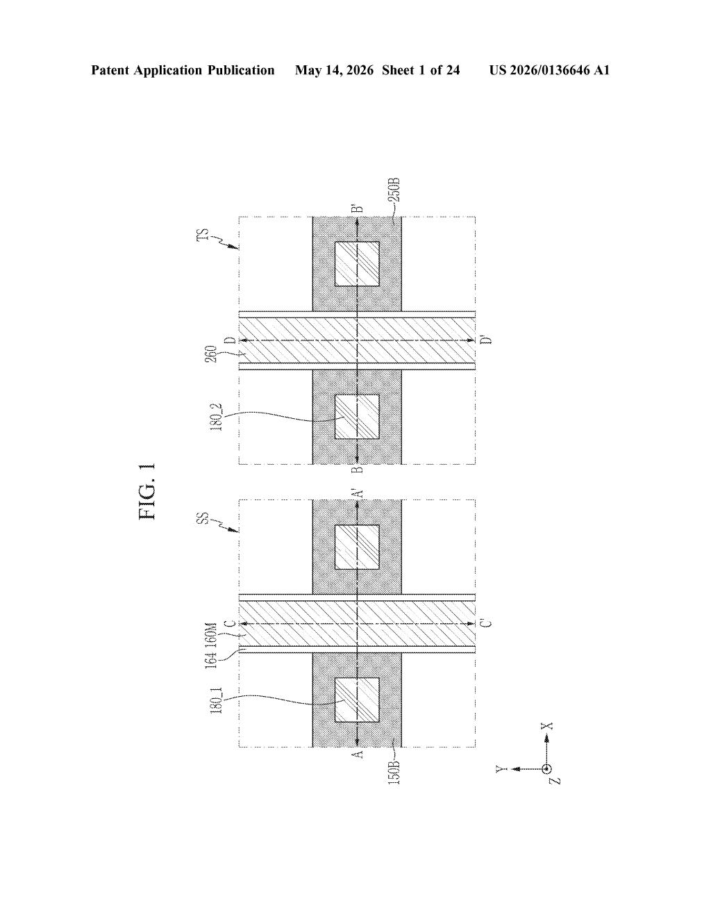
How the PN junction sits between Samsung's sheet stacks
The patent describes a semiconductor device built from two vertically stacked "sheet structures" — each one a series of alternating semiconductor layers (think of them as ultra-thin silicon ribbons, similar to the nanosheet or gate-all-around transistor architectures already in production).
The key innovation is the PN junction structure sandwiched between the lower sheet structure and the upper sheet structure. A PN junction (the same basic principle used in diodes and every transistor ever made) is formed by placing a P-type doped layer — where positive charge carriers dominate — directly against an N-type doped layer — where negative charge carriers dominate. This junction acts as an electrical boundary that can be precisely controlled.
Each sheet structure also has semiconductor patterns on its sides, which are the contact points for source/drain regions — the parts of a transistor where current enters and exits. The architecture essentially gives you:
- A bottom transistor stack (lower sheet structure)
- A top transistor stack (upper sheet structure)
- A PN junction between them acting as an isolation and control layer
This approach is closely related to complementary field-effect transistor (CFET) research, where N-type and P-type transistors are stacked vertically instead of placed side by side — a major frontier in sub-2nm chip design.
What this means for next-generation Samsung chip density
The semiconductor industry has been trying to keep Moore's Law alive by going vertical. CFET-style stacking — putting N-type and P-type transistors on top of each other — is seen as the next major step after gate-all-around (GAA) transistors. Samsung, TSMC, and Intel are all racing toward it. This patent puts Samsung on record with a specific architectural approach to that transition, using a PN junction as the boundary layer between stacked transistor tiers.
For you as a consumer, this is the kind of deep foundational work that eventually shows up as faster, more power-efficient chips in phones, AI accelerators, and data center processors. It won't ship tomorrow — CFET is still largely in research — but the companies that nail the architecture now will own the process nodes of the late 2020s.
This is exactly the kind of patent you'd expect from Samsung's advanced process R&D team right now — serious foundational work on CFET-adjacent transistor stacking that maps directly to sub-2nm competition with TSMC and Intel. It's not flashy, but stacking transistors vertically with a controlled PN junction boundary is a genuine technical challenge, and filing this signals Samsung is actively working the problem. Worth tracking if you follow semiconductor process technology.
Get one Big Tech patent every Sunday
Plain English, intelligent commentary, no hype. Free.
Editorial commentary on a publicly published patent application. Not legal advice.