Samsung Patents a Stacked-Layer Transistor Design for Advanced Semiconductors
Samsung is patenting a transistor architecture where stacked semiconductor layers deliberately vary in thickness — a structural tweak that could influence how current flows through next-generation chips built at extreme scales.
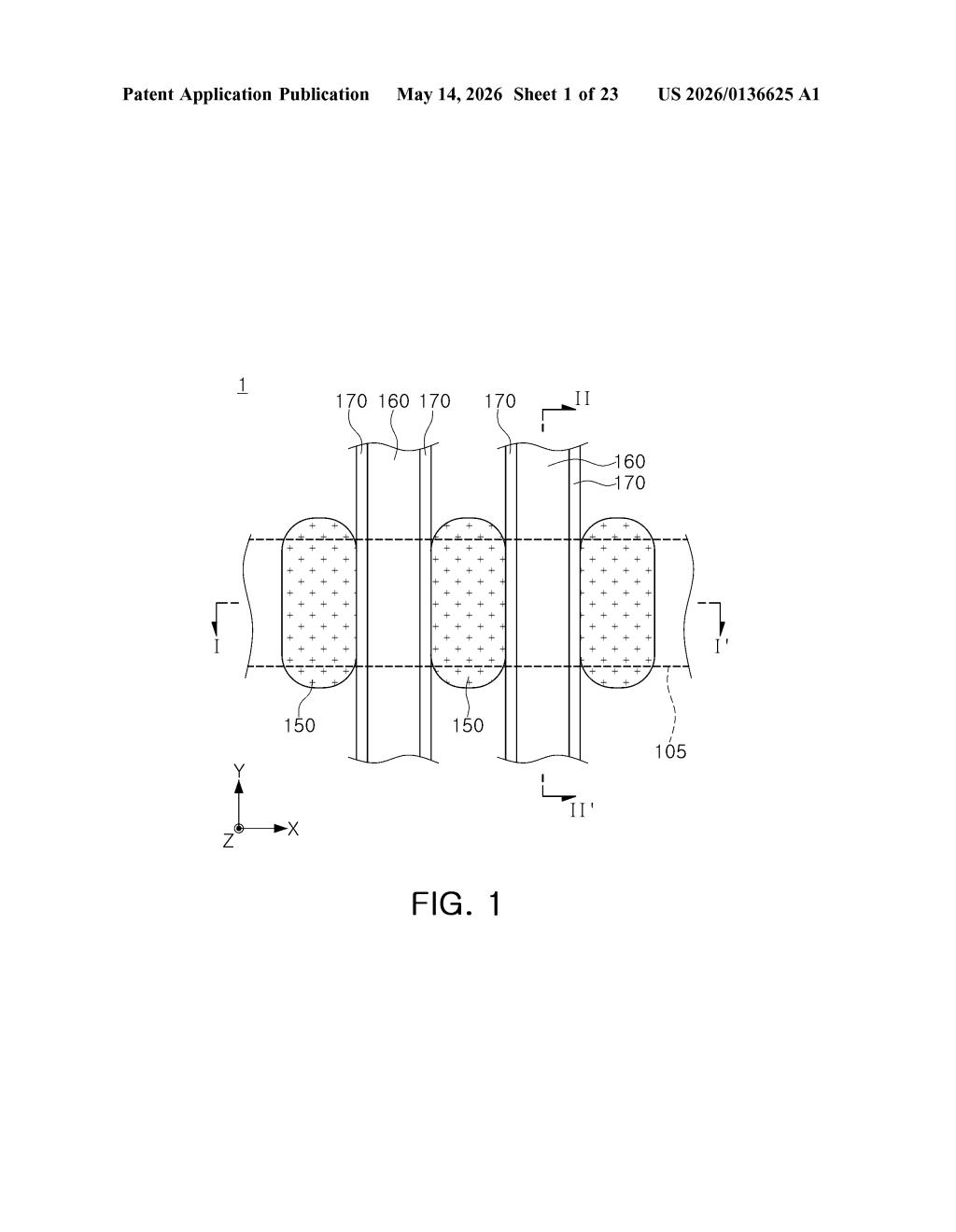
What Samsung's stacked transistor layers actually do
Imagine the transistors inside a chip as tiny switches that control electricity. As chips get smaller and more powerful, engineers can't just shrink those switches in simple ways — they have to rethink their shape entirely.
Samsung's patent describes a design where multiple thin semiconductor layers are stacked vertically, one above another, like a small pile of ribbon-shaped wires. Crucially, the topmost layer is thicker than the ones below it. A single gate electrode wraps around all of these layers at once, controlling them together.
This kind of architecture is closely related to what the chip industry calls "gate-all-around" (GAA) transistors — the next step beyond today's FinFET designs used in modern smartphones and laptops. Samsung is one of the leading fabs pushing GAA into production, and this patent is a window into how they're fine-tuning the geometry.
How Samsung arranges the semiconductor layers and gate
The patent describes a nanosheet or multi-bridge-channel transistor — a type of gate-all-around (GAA) device where the "channel" (the path electrons travel) is formed by several thin semiconductor sheets stacked vertically instead of a single fin or planar surface.
Key structural elements include:
- Active region: A strip of semiconductor material running along the substrate in one direction, forming the foundation for the transistors.
- Stacked semiconductor layers: Multiple horizontally oriented sheets sitting above the active region, separated vertically from each other. The uppermost layer is intentionally thicker than the lower layers — a non-uniform stacking approach.
- Gate structure: A gate electrode that wraps around (surrounds) each individual semiconductor layer — the defining feature of a GAA transistor, giving the gate more electrostatic control over the channel than older designs.
- Spacer structure and source/drain regions: Insulating spacers sit on both sides of the gate, while source and drain contacts touch all the stacked semiconductor layers simultaneously.
The non-uniform thickness — thicker on top — is the distinguishing detail. Varying layer thickness can help balance electrical characteristics across the stack, since the top and bottom layers experience slightly different mechanical stress and electrostatic environments during fabrication.
What this means for Samsung's chip scaling roadmap
GAA transistors are the architecture Samsung, TSMC, and Intel are all racing to commercialize at the 2nm and below nodes. Samsung began volume production of its 3nm GAA process (SF3) in 2022, and refinements like this patent speak directly to the engineering challenges of making those transistors reliable and performant at scale. The non-uniform layer thickness detail suggests Samsung's engineers are actively tuning GAA geometry to compensate for real-world fabrication imperfections or to optimize drive current.
For you as a consumer, GAA progress means future chips in phones, laptops, and AI accelerators can pack more transistors into the same area without burning more power — the foundation of every performance leap you've come to expect from new silicon generations.
This is a fairly narrow structural patent covering a specific nanosheet transistor geometry — it's not a conceptual leap, it's manufacturing-level refinement. That said, GAA transistor patents from Samsung right now are directly connected to active production processes, so this isn't abstract research. It's the kind of incremental detail that separates working chips from ones that fail yield tests.
Get one Big Tech patent every Sunday
Plain English, intelligent commentary, no hype. Free.
Editorial commentary on a publicly published patent application. Not legal advice.