Samsung Patents an Improved Phase-Shift EUV Mask for Chip Patterning
Samsung is patenting a redesigned mask for extreme ultraviolet lithography — the process that etches today's most advanced chips — with a clever height-difference trick that could sharpen pattern edges and widen manufacturing tolerances.
What Samsung's EUV mask redesign actually does
Imagine trying to project an incredibly detailed shadow onto a surface using a stencil, but the light is so powerful and short-wavelength that even tiny imperfections in the stencil create blurry edges. That's essentially the problem chip makers face with extreme ultraviolet (EUV) lithography, which is how cutting-edge processors and memory chips get their impossibly fine circuit patterns.
Samsung's patent describes a smarter mask — the reusable 'stencil' that defines the chip's circuit pattern — where the areas not meant to transfer a pattern sit physically lower than the areas that are. This height difference, combined with a phase-shift structure, manipulates how EUV light reflects off different parts of the mask.
The result is better contrast between the 'print this' and 'don't print this' zones. In manufacturing terms, that translates to sharper circuit lines and a bigger margin for error, meaning fewer defective chips coming off the production line.
How Samsung's phase-shift layer stack controls EUV light
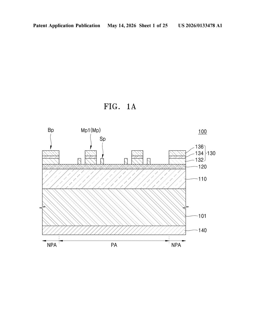
The mask sits at the heart of the EUV exposure system and works in reflection mode — unlike older lithography masks that let light pass through, EUV masks bounce the light back toward the wafer below.
The patented design layers up like this:
- A substrate (the base) carries a reflective surface underneath.
- A multi-reflective layer (alternating molybdenum and silicon layers, the standard EUV mirror stack) sits on top of the substrate to amplify reflected EUV light.
- A phase-shift structure on top of that contains two types of zones: transfer patterns (the features you want printed on the chip) and non-transfer patterns (the background areas you don't).
The key innovation is geometric: the non-transfer pattern's top surface is intentionally recessed — sitting closer to the substrate — compared to the taller first transfer pattern. This height differential causes EUV light reflecting off those two zones to arrive slightly out of phase with each other (think of two ripples in a pond canceling out at the edges). That phase cancellation suppresses stray light at pattern boundaries, producing sharper printed features.
The transfer pattern itself uses a multi-layer structure, giving Samsung design flexibility to tune phase and reflectivity independently for different feature types on the same mask.
What this means for Samsung's advanced chip manufacturing
EUV lithography is the bottleneck technology for manufacturing chips at 3nm, 2nm, and below — the nodes where Samsung competes directly with TSMC and Intel Foundry. Patterning margin (how much process variation a mask can tolerate before producing bad chips) is one of the tightest constraints at these scales. A mask design that widens that margin, even slightly, can meaningfully improve yield — which is everything in a business where a single fab line costs billions of dollars.
For you as a consumer, better EUV mask designs are a quiet but direct path to cheaper, faster, more power-efficient chips in future phones and laptops. This is deeply unsexy foundry engineering, but it's exactly the kind of incremental improvement that compounds into generational chip performance gains.
This is niche, deep-stack semiconductor process IP — not a product patent, not an AI angle, just serious lithography engineering. Samsung's foundry business is under real competitive pressure from TSMC, and patents like this represent the unglamorous trench warfare of advanced node manufacturing. Worth paying attention to if you track semiconductor supply chain or EUV ecosystems; easy to skip if you don't.
Get one Big Tech patent every Sunday
Plain English, intelligent commentary, no hype. Free.
Editorial commentary on a publicly published patent application. Not legal advice.