
Sony Patents a Camera Component That Measures Distances With Greater Precision
Sony is working on a way to squeeze an ultra-sensitive light detector and its supporting electronics onto a single chip without them interfering with each other, a design challenge that matters a lot for anything that needs to measure distance with a pulse of light.
What Sony's combined light-sensor chip actually does
Imagine a speed camera that works by firing an invisible laser pulse and timing how long it takes to bounce back. The sensor that catches that returning light has to be incredibly sensitive, sensitive enough to detect a single photon. That kind of sensor is called a SPAD (a Single-Photon Avalanche Diode), and it's already used in smartphone cameras, LiDAR systems, and face-recognition hardware.
The problem is that a SPAD operates under a very high internal voltage, and if you put regular electronics right next to it on the same chip, the electrical noise can bleed across and cause errors. Sony's patent describes a design where the SPAD and its neighboring components sit on the same base layer but are separated by an insulating barrier, keeping each part electrically isolated.
The goal is a cleaner, more compact chip that can measure distances accurately without needing separate components spread across multiple pieces of silicon.
an avalanche diode that is provided in a first region of a first base, and amplifies a carrier generated by an incident photon …
Translation: A special light-sensing diode boosts the signal created when a single particle of light hits it.
How the insulating barrier keeps the detector stable
The patent describes a photodetector built around a SPAD (Single-Photon Avalanche Diode), a type of sensor that can detect individual photons and produce a measurable electrical pulse. SPADs are the core of time-of-flight distance measurement, the system fires a laser, the SPAD catches the reflected light, and the time gap tells you how far away an object is.
The core engineering challenge Sony is addressing: SPADs require a high reverse-bias voltage to work, which creates electrical noise. Putting other circuit elements (amplifiers, signal processors, timing circuits) right next to the SPAD on the same piece of silicon risks interference.
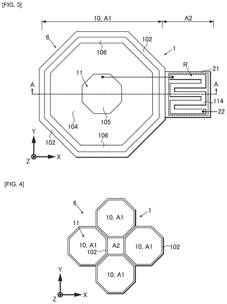
Sony's solution is an insulating isolator placed between the SPAD's region and the neighboring components' region on the same base. Think of it as a firewall built directly into the silicon. The two zones sit side by side in the same flat plane of the chip, but the insulating layer prevents electrical signals from leaking between them.
Key elements of the design include:
- A first region housing the SPAD (the light-sensing avalanche diode)
- A second region for other circuit elements, placed adjacent in the same chip layer
- An insulating isolator between the two regions for electrical separation
… an insulating isolator that is provided between the first region and the second region, and at least electrically isolates the SPAD and the one or more elements from each other …
Translation: A barrier wall keeps the main light sensor electrically separated from surrounding circuitry.
What this means for cameras and depth-sensing devices
Distance sensing is already in your smartphone (for portrait-mode depth maps and Face ID), your car (for parking sensors and driver-assist systems), and industrial robots. All of these increasingly rely on SPADs because they're faster and more sensitive than older light sensors. Fitting the SPAD and its supporting circuitry onto one compact, well-isolated chip makes the whole system smaller, cheaper, and potentially more power-efficient.
Sony Semiconductor Solutions is one of the world's largest image sensor manufacturers, supplying chips to Apple, Samsung, and many camera makers. A cleaner SPAD integration could find its way into next-generation LiDAR modules, AR glasses, or medical imaging gear where precise depth measurement at low power is a priority.
This is incremental silicon engineering rather than a conceptual leap, the idea of isolating noisy components on a chip is well established. That said, Sony filing it signals active work on next-generation SPAD-based sensors, and given the company's dominant position in the image sensor market, even a modest integration improvement here could ripple across a huge number of devices.
There are more where this came from
We read every patent application Big Tech publishes and send you the ones worth knowing. Plain English, free, every week.
The drawings
55 drawing sheets from US 2026/0227494 A1 · click any drawing to enlarge


Want this weekly breakdown for a company we don't cover? Patentlyze Pro →
Be the first to weigh in