
Patent: Two Types of Camera Pixels Work Together for Faster, Richer Video
Sony is designing a camera sensor where some pixels act as a rapid-response early-warning system, telling the rest of the sensor how to behave before a full image is even captured.
What Sony's two-tier camera sensor actually does
Imagine you're filming a street scene and a car suddenly swerves into frame. A normal camera sensor treats every pixel equally, so it takes a moment to catch up to fast changes in light or motion before adjusting settings. Sony's patent describes a smarter split.
The sensor divides its pixels into two groups. One group is built for speed, these pixels react very quickly to changes in the scene, even if they don't produce detailed, colorful images on their own. The other group captures the full, rich color frames you'd actually want to save or stream.
The fast pixels work like scouts: they continuously read the scene and tell the camera's processing unit what's happening right now. Based on that, the system adjusts how it handles the slower, higher-quality pixels. The result is a sensor that can respond to fast-moving or rapidly changing scenes without making the whole camera slower.
… a first subset of pixels and a second subset of pixels, where pixels of the first subset of pixels are capable to generate pixel signals faster and preferably with less spatial resolution than pixels of the second subset of pixels …
Translation: The sensor splits pixels into two groups where one works faster with lower detail.
How the fast pixels steer the slow color pixels
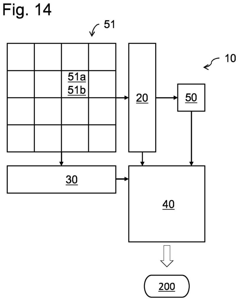
The patent describes a sensor device built around two distinct subsets of pixels on the same chip.
- First subset (fast pixels): These pixels are designed to generate signals quickly, trading away spatial resolution (fine detail) for speed. Think of them as low-resolution but extremely reactive sensors embedded across the pixel array.
- Second subset (standard pixels): These capture full color frames at normal resolution, the kind of image data that ends up in your video file.
- Control unit: A dedicated controller continuously reads signals from the fast pixels and uses that information to switch the operating modes of the main processing unit in real time.
The key idea is that the fast pixels act as a continuous, low-latency (near-instant) feed that the system uses to make decisions, for example, switching exposure modes, triggering high-dynamic-range processing, or adjusting how frames are buffered, before the slower color pixels have even finished their current frame cycle.
This is essentially an on-chip feedback loop: the sensor monitors itself through the fast pixel layer and adapts its processing pipeline accordingly, without waiting for software running on a separate processor to issue instructions.
… a control unit that is configured to receive pixel signals from the first subset of pixels and to control operation modes of the processing unit based on the received pixel signals from the first subset of pixels …
Translation: A control unit uses data from the fast pixels to adjust how the processor handles video.
What this means for video cameras and future Sony products
For video cameras, the gap between when something happens and when the sensor reacts is a longstanding problem. Fast action, sudden lighting changes, or high-contrast scenes can all catch a sensor mid-cycle, producing blown-out, blurry, or poorly exposed frames. By embedding a fast-response layer directly into the pixel array, Sony's approach moves that reaction time as close to the physics of light as possible.
Sony Semiconductor Solutions supplies image sensors to a wide range of camera makers, including Sony's own camera division. A sensor architecture like this could improve slow-motion video capture, surveillance cameras, or any application where scene dynamics change faster than a traditional frame rate allows. It could also reduce the processing burden on external chips, since the sensor itself handles more of the adaptive logic.
This is a genuinely interesting hardware-level approach to a real problem in video capture. Instead of throwing more computing power at fast-changing scenes after the fact, Sony is baking the feedback loop into the sensor itself. Whether it shows up in a consumer camera or stays in industrial and automotive imaging is hard to say, but the underlying logic is solid.
There are more where this came from
We read every patent application Big Tech publishes and send you the ones worth knowing. Plain English, free, every week.
The drawings
24 drawing sheets from US 2026/0230718 A1 · click any drawing to enlarge


Want this weekly breakdown for a company we don't cover? Patentlyze Pro →
Be the first to weigh in