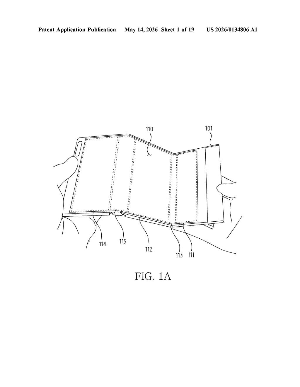
Samsung Patents a Display Panel That Senses Its Own Deformation
Samsung is exploring a way to embed touch and pressure sensing directly into the structure of an OLED display — not as a separate layer on top, but woven into the very material that defines where each pixel lives.
What Samsung's pressure-sensing OLED panel actually does
Imagine pressing on your phone's screen and it doesn't just register where your finger is, but how hard you're pushing — and then uses that to trigger different actions. That's the idea behind this Samsung patent.
Instead of adding a dedicated pressure sensor underneath the display, Samsung wants to use a conductive material embedded in the pixel definition layer (PDL) — the thin structure that separates individual pixels in an OLED screen. When you press or bend the display, that conductive material deforms slightly, changing its electrical properties. The display driver chip picks up on this change and reports it to the processor.
The processor then decides what to do with that information — launching a function, adjusting behavior, or responding to a bend gesture. It's a clever way to add sensing capability without bolting on extra hardware.
How conductive material in the PDL detects screen deformation
OLED displays are built from millions of tiny sub-pixels, each containing a light-emitting diode. Between those sub-pixels sits the pixel definition layer (PDL) — essentially a thin insulating wall that keeps the pixels separated and properly shaped. Samsung's patent embeds conductive materials into portions of that PDL.
When the display panel is deformed — bent, pressed, or flexed — those conductive materials deform too, altering their electrical state. The display driver circuitry (the chip already responsible for powering each pixel) monitors the electrical condition of those conductive traces and transmits that data to the main processor.
The processor then interprets the deformation data and executes a corresponding function. The claim is intentionally broad — "a function corresponding to at least partial deformation" — which could mean anything from a haptic response to a UI shortcut to detecting whether a foldable device is open or closed.
- PDL with embedded conductors — the sensing element, built into existing display structure
- Display driver circuitry — doubles as the sensing data relay, no separate sensor IC needed
- Processor + memory — interprets the deformation state and triggers actions
What this means for foldables and pressure-touch displays
The interesting engineering bet here is co-opting existing display infrastructure for sensing. Adding a dedicated pressure or bend sensor to a thin foldable device costs space, power, and manufacturing complexity. If Samsung can route sensing through the display driver chip that's already present, that's a real bill-of-materials win — especially for ultra-thin foldables where every micron matters.
For foldable phones like the Galaxy Z Fold and Z Flip lines, knowing the precise deformation state of the hinge area could unlock smarter app-switching, more reliable open/closed detection, or even new squeeze gestures. It could also apply to rollable or flexible display concepts Samsung has shown publicly. The question is whether the sensitivity and reliability of PDL-embedded conductors holds up at scale.
This is a quiet but genuinely clever piece of integration engineering — Samsung is essentially asking 'what if the display told us when it was being bent, without a separate sensor?' For foldable devices, that's a real problem worth solving, and routing it through the existing display driver rather than adding hardware is the kind of cost-conscious design that actually ships. Worth watching as foldable lineups get thinner.
Get one Big Tech patent every Sunday
Plain English, intelligent commentary, no hype. Free.
Editorial commentary on a publicly published patent application. Not legal advice.