
Samsung Patents a Layered Wiring Layout That Keeps Touchscreens Reading Your Taps Accurately
Every time a touchscreen misreads your tap, there's a good chance the culprit is where two sensing wires cross inside the panel. Samsung's latest patent targets exactly that junction.
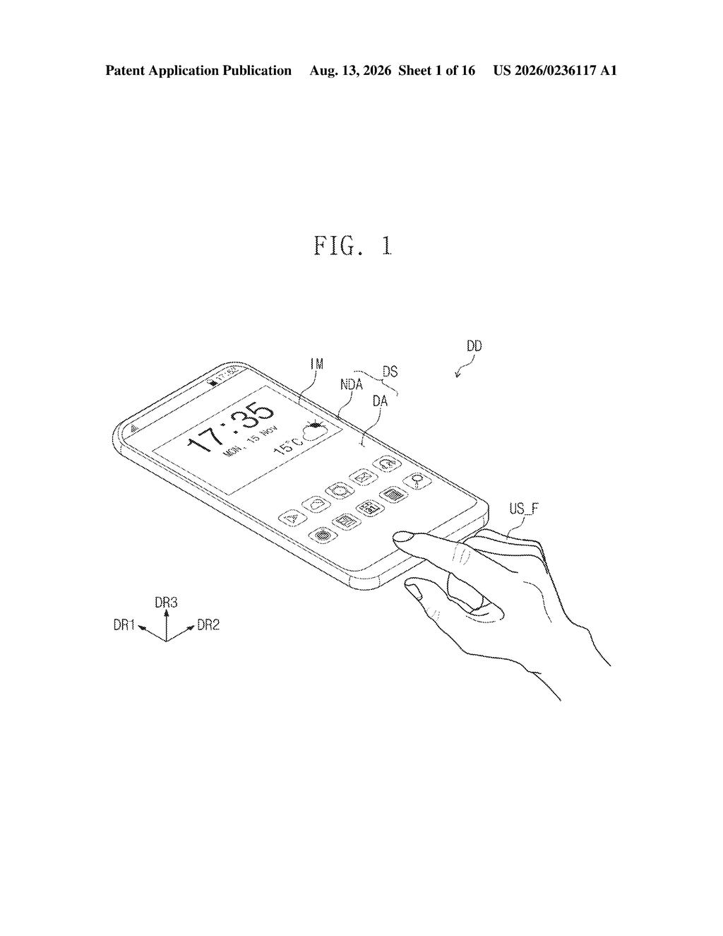
What Samsung's crossing-wire touch fix actually does
Every time you tap your phone awake, the touchscreen's internal wiring has to figure out precisely where your finger landed. That job gets harder at the spots where horizontal and vertical sensor lines cross each other, because those intersections can cause interference that throws off the reading.
Samsung's patent describes a way to wire those crossing points using a combination of stacked wire layers and carefully varied wire widths. The idea is to route signals through a double-layer conductor where they need strength, then hand off to thinner single-layer wires as they fan out, reducing the chance that two crossing signals confuse each other.
The practical result, if it works as described, is a touchscreen that stays accurate even as the internal wiring gets more tightly packed. That matters most as Samsung pushes displays thinner and folds them, since both trends leave less room for the sensor grid underneath.
… a first multi-layer line electrically connected to the second sensing electrode, the first multi-layer line including a first line and a second line disposed over the first line …
Translation: The design uses a stacked wiring structure where one wire sits directly on top of another to connect to the sensor.
How the stacked lines and width shifts handle signal conflicts
The patent covers an input sensing part, which is the layer inside a display panel that detects where and how your finger touches the screen. It has two sets of electrodes: one running roughly horizontally and one running vertically, and they have to cross without electrically shorting together or creating noise.
The filing introduces a specific wiring architecture to manage those crossings:
- A first multi-layer line: two conductive lines stacked on top of each other, connected to one set of sensing electrodes. Stacking them reduces electrical resistance, which keeps signals strong over longer runs.
- A first single-layer line: a thinner wire that branches off one of those stacked layers and routes the signal sideways.
- A second single-layer line: a wire sitting in a different physical layer of the panel, connected to the first single-layer line, but with a different width.
The geometry matters: the patent specifies that the single-layer lines include a straight section and a bent section, and that a nearby sensing line narrows at the bend point. Varying the widths at those bends is the mechanism for controlling how the signals behave near each other, limiting parasitic capacitance (the unwanted electrical coupling that makes one wire accidentally pick up a signal from its neighbor).
In short, the design uses layer stacking for conductivity and width tuning for interference control, two tools working at different scales inside the same sensor grid.
… a second single-layer line that is disposed in a different layer from the first single-layer line and electrically connected to the first single-layer line and that has a different line width from the first single-layer line.
Translation: The patent describes connecting wires of different thicknesses across separate layers to improve the touchscreen layout.
What this means for touch accuracy in thin Samsung displays
Touch accuracy problems tend to be invisible until they aren't: the mis-tap that opens the wrong app, the stylus stroke that skips, the pinch-to-zoom that stutters. Those failures often trace back to interference inside the sensor layer, and they get harder to avoid as manufacturers pack more pixels and thinner bezels into panels. A wiring architecture that reduces cross-talk at intersections directly lowers the chance a user runs into those moments.
For Samsung specifically, the stakes are higher than for a flat-phone maker. Foldable displays flex the sensor layer repeatedly, and the tighter bend radius at the fold is exactly where interference-prone wire crossings are hardest to manage. The latest Big Tech patents in display and touch-sensing show a consistent push toward thinner, foldable, and rollable panels, and Samsung's multilayer wiring approach fits squarely into that engineering pressure.
This patent addresses something real: touch-accuracy degradation at sensor-line crossings is a documented engineering headache that gets worse as displays shrink and flex. The solution, mixing stacked conductors with width-varied single-layer branches, is specific enough to suggest Samsung's display engineers ran into a concrete problem and designed around it. A user who benefits from this work will never know it happened, which is exactly the point: the fix shows up as taps that land where they're supposed to, even on a folded or paper-thin panel.
There are more where this came from
We read every patent application Big Tech publishes and send you the ones worth knowing. Plain English, free, every week.
The drawings
16 drawing sheets from US 2026/0236117 A1 · click any drawing to enlarge


Want this weekly breakdown for a company we don't cover? Patentlyze Pro →
Be the first to weigh in