
Sony Patents a Two-Layer Stacked Chip for Compact LiDAR Distance Sensing
Sony Semiconductor is trying to shrink a LiDAR sensor down to a two-layer silicon sandwich — putting the laser emitter and light receiver on one chip, and the processing circuitry on a second chip bonded directly beneath it.
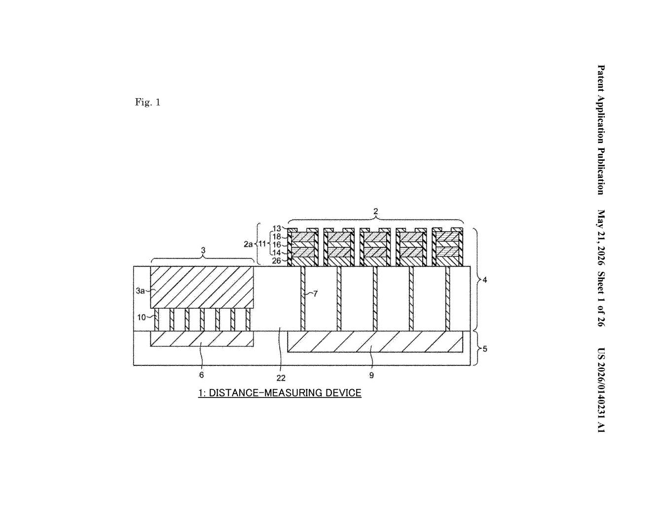
What Sony's stacked LiDAR sensor chip actually does
Imagine your phone trying to measure how far away your face is to unlock itself, or a robot trying to judge the distance to an obstacle. That kind of depth-sensing usually requires a device that shoots out pulses of light, waits for them to bounce back, and times how long the round trip takes. The problem is that doing all of that — emitting, receiving, and processing — traditionally needs separate components, which takes up space and drains power.
Sony's patent describes a sensor that squeezes all of this onto two stacked chips bonded together. The top chip, made of a Group-IV material (think silicon or germanium — the basic semiconductors your processor is built from), holds both the laser emitter and the light receiver side by side. The bottom chip handles the electronic readout — turning the raw light signal into a distance number.
By stacking these layers instead of spreading them across a circuit board, you get a smaller footprint, fewer connections that can fail, and — according to the filing — lower power consumption. It's the same philosophy behind stacked memory chips, just applied to depth sensing.
How the two-substrate stack splits light and logic
This patent covers a time-of-flight (ToF) distance-measuring device built as a two-substrate stack. ToF works by sending out a short pulse of light and measuring how long it takes to return after bouncing off an object — the longer the round trip, the farther away the object is.
The key architectural choice here is monolithic integration on a Group-IV substrate. Group-IV materials (silicon, germanium, silicon-germanium alloys) are the workhorses of conventional chip fabrication. By building both the light-emitting portion (the laser or LED that fires pulses) and the light-receiving portion (the photodetector that catches the reflected signal) on the same piece of Group-IV material, Sony avoids the hybrid assembly that typically involves bonding a compound semiconductor laser (like InGaAs or GaAs) onto a silicon base — a step that adds cost and complexity.
The second substrate is laminated directly onto the first and carries the readout circuit — the analog-to-digital conversion and timing logic that interprets the photodetector's signal as a distance value.
- First substrate (Group-IV): integrates light emitter + light receiver together
- Second substrate: stacked below, handles electronic readout and signal processing
- Result: smaller package, fewer off-chip connections, lower power draw
What this means for small, low-power depth cameras
Miniaturization is the central pressure in depth-sensing right now. Automotive LiDAR, AR/VR headsets, industrial robots, and even consumer smartphones all want accurate distance measurement in an ever-shrinking form factor. Today's solutions often involve hybrid assemblies — a laser chip from one vendor, a detector from another, glued or wire-bonded together. That approach has real limits in size, yield, and cost.
Sony Semiconductor is one of the world's largest image sensor manufacturers, and this filing signals a push to own more of the depth-sensing stack in silicon. If they can bring Group-IV-based emitters up to production quality, the stacked architecture here would let them build a full ToF sensor the same way they already build stacked CMOS image sensors — with well-understood fab processes and tight vertical integration. That's a meaningful cost and supply-chain advantage.
This is a solid, focused engineering patent rather than a flashy concept. Sony Semiconductor already dominates stacked CMOS image sensors, and this looks like a deliberate extension of that stacking expertise into ToF depth sensing. The real question is whether Group-IV-based light emitters can hit the performance needed for demanding applications like automotive LiDAR — but for short-range use cases like face unlock or gesture sensing, this architecture looks well-suited.
Get our take in your Top Stories
Liked this breakdown? Add Patentlyze as a preferred source on Google, and our plain-English take shows up more often in your Top Stories the next time Sony patent news breaks.
There are more where this came from
We read every patent application Big Tech publishes and send you the ones worth knowing. Plain English, free, every week.
Want this weekly breakdown for a company we don't cover? Patentlyze Pro →