
Samsung Patents a Design That Keeps Stacked Memory Chips From Shifting Under Pressure
Samsung is patenting a specific physical layout for high bandwidth memory chips that places non-functional 'dummy' structures alongside the electrical contact points where stacked chip layers meet. It's a manufacturing detail, but the kind that separates reliable chips from ones that crack under pressure.
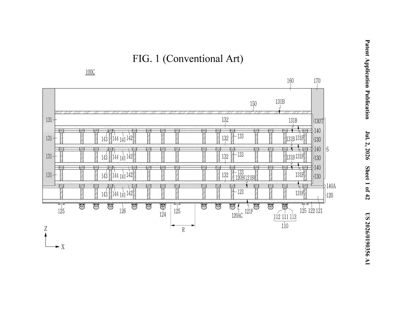
What Samsung's stacked memory chip layout actually does
Imagine stacking several thin wafers of memory on top of each other, like a tiny multi-story building. The floors have to connect perfectly, or the whole structure becomes unreliable. That's essentially what high bandwidth memory (HBM) is, and it's the type of memory used in AI chips and high-performance computers.
The tricky part is making sure those floors are level and stable. Samsung's patent describes a base layer (the ground floor) whose top surface is divided into two zones: a central area and a surrounding ring. The central area gets filled with dummy structures, which are placeholder shapes that don't carry any electrical signal. The outer ring gets the real bump connections, the tiny solder points that link the memory stack to whatever chip it's attached to.
Those dummy structures aren't decoration. They help keep the surface flat and mechanically even during manufacturing, so the bump connections land correctly and the chip layers above don't warp or crack.
How the dummy patterns and bump layout fit together
The patent describes a high bandwidth memory (HBM) architecture built around a base die (think of it as the foundation chip) that has two distinct surface zones.
- First region (center): Populated with one or more dummy patterns, non-conductive filler structures that serve no electrical function but provide mechanical support and surface uniformity.
- Second region (outer ring): Contains the active bump patterns, the physical solder contacts that carry signals and power between the memory stack and the host processor or logic chip below.
- Semiconductor stack (opposite surface): Multiple core dies (the actual memory layers) are bonded to the back of the base die, forming the full HBM module.
The dummy patterns matter most during fabrication. When chips are bonded together under heat and pressure, uneven surfaces cause misalignment and mechanical stress. Filling the center zone with dummy structures keeps the surface topology consistent across the die, so the bump contacts in the outer ring can be applied and compressed evenly. This reduces the risk of cracking, delamination, or electrical opens in the finished part.
The claim is deliberately broad, covering any HBM where the base die's first surface has this center-plus-ring zone arrangement with dummy patterns in the center.
What this means for high-end AI and server memory chips
HBM is the memory that powers AI accelerators like Nvidia's H100 and AMD's Instinct series, and demand for it is intense. Manufacturing yield, meaning how many chips come out of the fab working correctly, is one of the biggest cost levers in this market. A layout technique that reduces warping or contact failures during bonding can meaningfully improve yield without changing the underlying chip design.
For you as a consumer, this doesn't change anything directly. But for data centers buying thousands of AI servers, even a small yield improvement translates to lower chip costs over time. Samsung is one of the few companies that makes HBM at scale alongside SK Hynix and Micron, so packaging and bonding patents like this are part of how they compete.
This is a narrow manufacturing-process patent, not a chip architecture breakthrough. It's the kind of incremental packaging detail that semiconductor companies file constantly to protect their fab recipes. Worth knowing about if you follow HBM supply chain dynamics, but there's no headline product angle here.
Get our take in your Top Stories
Liked this breakdown? Add Patentlyze as a preferred source on Google, and our plain-English take shows up more often in your Top Stories the next time Samsung patent news breaks.
There are more where this came from
We read every patent application Big Tech publishes and send you the ones worth knowing. Plain English, free, every week.
Want this weekly breakdown for a company we don't cover? Patentlyze Pro →