Samsung Patents a Hybrid SEM Imaging Method for Cleaner Chip Inspection
Getting a sharp, low-noise image of a chip wafer under an electron microscope is a classic tradeoff: slow the scan down and you get better signal, but throughput tanks. Samsung's new patent tries to sidestep that tradeoff entirely by borrowing clarity from a different image altogether.
What Samsung's SEM noise-reduction trick actually does
Imagine trying to photograph a tiny circuit in bad lighting. You can slow the camera shutter way down to let in more light — but then everything blurs if anything moves. Or you can shoot fast and get a sharp but grainy image. Chip inspection has the same problem: slow scans are detailed but slow production lines down; fast scans are quick but noisy.
Samsung's approach is to use two images instead of one. The real wafer gets a slow, careful scan that captures precise structural details. A reference sample — essentially a stand-in with the same layout — gets a fast, high-throughput scan. Then a combined image is built by pulling the shape and position data from the slow scan and the brightness and contrast data from the fast one.
The result is a clean, high-quality image without having to slow down every single wafer scan. It's a divide-and-conquer approach to a problem that normally forces a direct tradeoff.
How phase and amplitude data get stitched together
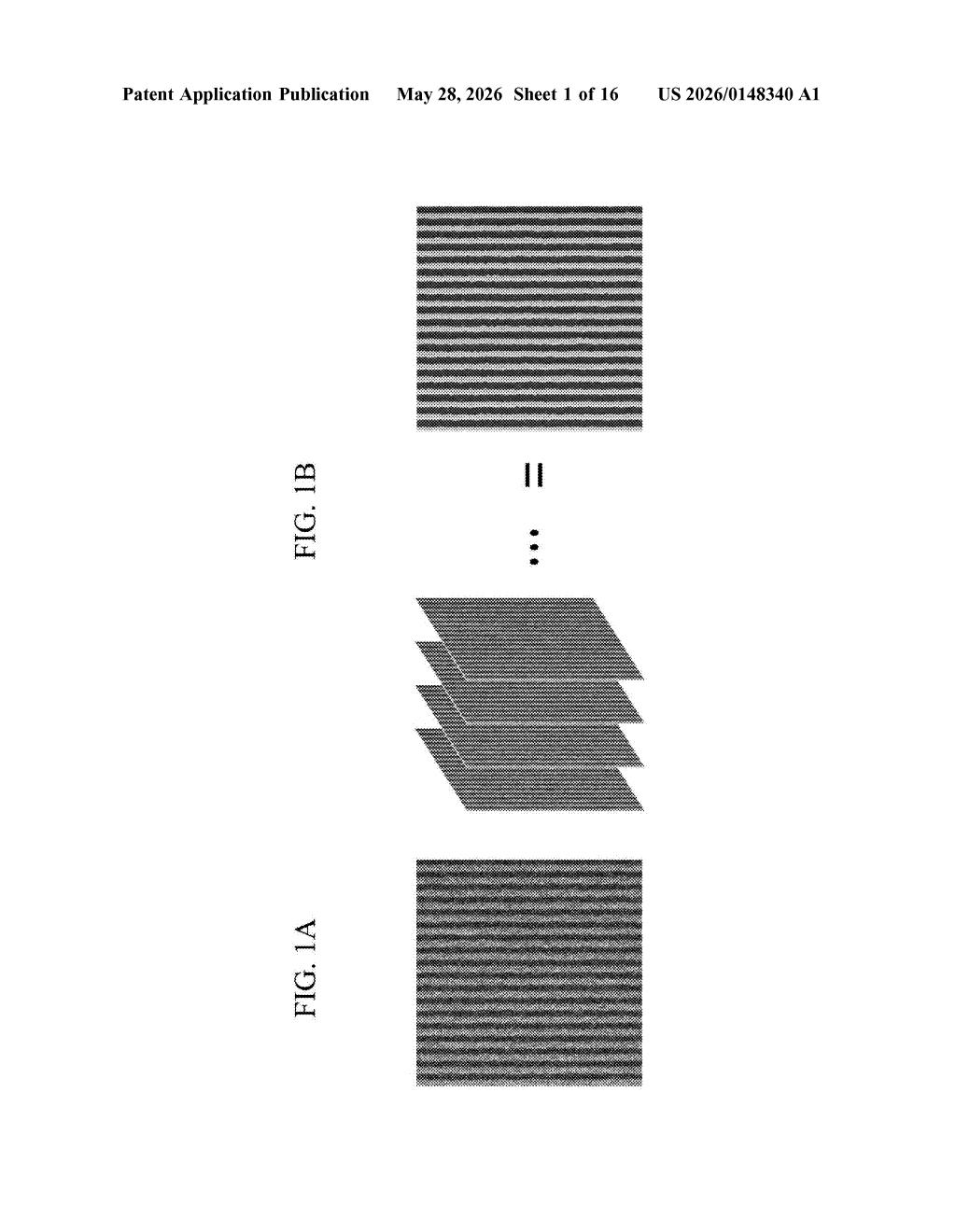
The patent describes a three-step imaging pipeline for a scanning electron microscope (SEM) — the kind of instrument used to inspect semiconductor wafers for defects at nanometer scale.
- First, the actual wafer sample (the thing you care about) is scanned at a low frame rate, which is slow but preserves structural information. This becomes the "first image."
- Next, a reference sample — a known-good or standard specimen with the same number of patterns — is scanned at a high frame rate. Fast scanning is noisier but gives you good amplitude (brightness/contrast) data.
- Finally, a second image is synthesized by combining the phase information from the first image (think: where the structures are and how they're shaped) with the amplitude information from the reference sample (think: how bright each feature should look). The result has a higher signal-to-noise ratio than either source alone.
The key constraint is that both images must contain the same number of patterns, which allows the phase and amplitude channels to be meaningfully matched and recombined.
What this means for wafer defect detection at scale
Semiconductor manufacturing yield depends heavily on catching defects early — and catching them requires clear images. If this technique holds up, it could let fabs run SEM inspections faster without sacrificing the image quality needed to spot nanometer-scale flaws. That's a meaningful win in a process where throughput directly impacts cost per wafer.
Samsung operates both a chipmaking foundry and its own fab lines, so any efficiency gain in inspection tooling has direct business value. This isn't a consumer-facing patent, but it sits squarely in the infrastructure that makes leading-edge chips possible.
This is a focused, practical patent aimed at a real bottleneck in chip manufacturing. It won't make headlines outside of semiconductor circles, but the underlying idea — decoupling phase and amplitude collection so you're not stuck optimizing for both simultaneously — is genuinely elegant. Worth watching if you follow Samsung's foundry ambitions.
Get one Big Tech patent every Sunday
Plain English, intelligent commentary, no hype. Free.
Editorial commentary on a publicly published patent application. Not legal advice.