Samsung Patents Deliberately Mismatched Light-Capturing Filters to Sharpen Phone Camera Photos
Most camera sensors are built on strict symmetry — every pixel filter is the same size and shape. Samsung's new patent breaks that rule on purpose, and the asymmetry may be the whole point.
What Samsung's lopsided pixel filter design actually does
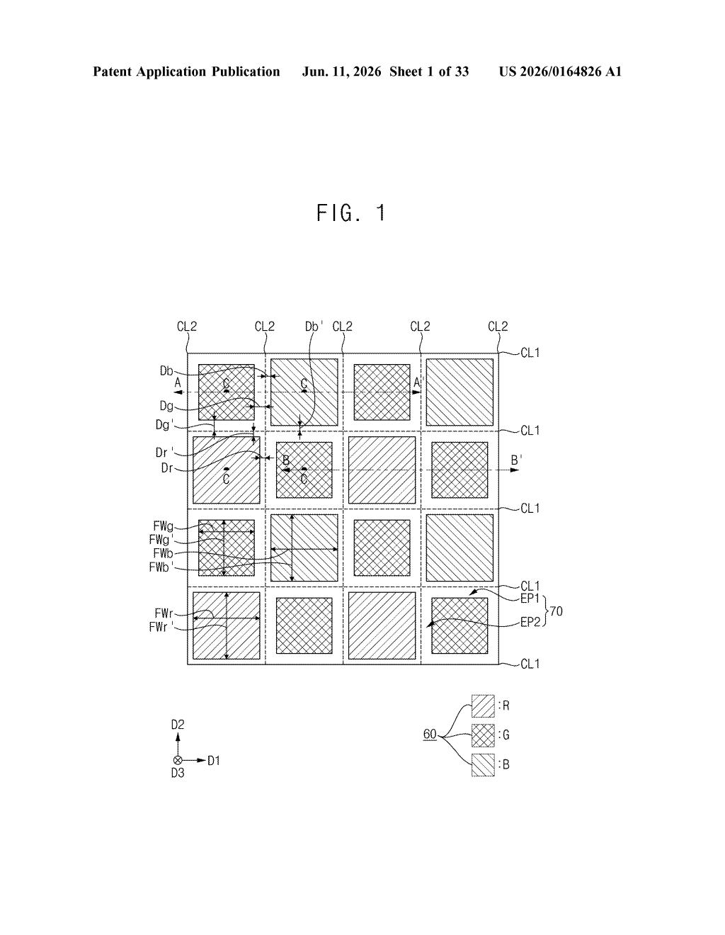
Think of a camera sensor as a grid of millions of tiny colored windows, each one capturing either red, green, or blue light. Normally those windows are identical in size, lined up perfectly like floor tiles. Samsung's patent describes a sensor where two neighboring color windows are intentionally different sizes — one extends further toward the dividing line between them than the other does.
That might sound like a manufacturing defect, but it's a deliberate design choice. By shifting how much space each filter occupies relative to its neighbor, Samsung can potentially control exactly where light lands on the light-catching layer underneath — which affects how accurately colors are recorded, especially in low-light or high-contrast situations.
The patent layers an optical structure on top of the filters, which likely means microlenses that focus incoming light. The asymmetric filter geometry underneath could work in tandem with that lens layer to steer light more precisely, reducing the color bleed between neighboring pixels that tends to degrade photo quality at high resolution.
How the asymmetric color filter geometry is laid out
The patent describes an image sensor built on a substrate (the base chip layer) containing at least two photodiodes (light-detecting elements) sitting side by side. On top of each photodiode sits a color filter — a microscopic layer that lets only one color of light through to the detector below.
The key claim is geometric: if you draw an imaginary center line exactly halfway between the two filters, the sidewall of the first filter is farther from that line than the sidewall of the second filter. In plain terms, one filter is wider relative to the gap between them than the other is. This is what the patent means by asymmetric placement.
- Substrate: the semiconductor base holding the photodiodes
- Color filters: microscopic colored layers (red, green, or blue) sitting above each photodiode
- Optical structure: a layer on top — likely microlenses — that focuses incoming light before it hits the filters
- Center line: a geometric reference point equidistant from the centers of both filters, used to define the asymmetry mathematically
The asymmetry is measured at a specific height within the filter stack, meaning the cross-sectional shape of the filters may taper or shift as you move up through the layers. This gives Samsung fine-grained control over how light is directed at each photodiode.
What this means for future Samsung camera sensors
As smartphone cameras pack more pixels into the same physical sensor area, each individual pixel shrinks — and smaller pixels are harder to isolate optically. Light meant for one pixel bleeds into its neighbor, degrading color accuracy and sharpness. Asymmetric filter geometry is one potential tool for compensating, letting engineers tune the light path at the pixel level rather than relying entirely on post-processing software.
For Samsung, which manufactures image sensors both for its own Galaxy devices and for other phone makers, this kind of low-level sensor architecture work is critical competitive territory. If the approach proves manufacturable at scale, it could feed into future high-resolution sensors where the physical limits of symmetric designs start to show.
This is a deep-stack semiconductor patent — the kind that rarely shows up in product announcements but quietly shapes what cameras can do three or four generations from now. The asymmetric filter concept is a real and non-obvious approach to a genuine problem in high-density sensor design, so it's worth taking seriously even if it reads like dry geometry on the surface.
Get one Big Tech patent every Sunday
Plain English, intelligent commentary, no hype. Free.
Editorial commentary on a publicly published patent application. Not legal advice.