Samsung Patents a Two-Layer 2D Semiconductor Channel Design for Next-Gen Chips
Samsung is working on a way to keep ultra-thin, atom-scale semiconductor channels from peeling off their substrates — a surprisingly tricky problem that's been slowing down the next generation of transistors.
What Samsung's dual-layer 2D semiconductor channel actually does
Imagine trying to stick a sheet of plastic wrap to a table so that only part of it is lightly attached — easy to work with — while the edges grip tight so the whole thing doesn't slide off. That's roughly the engineering challenge Samsung is tackling here with next-generation chip materials.
Modern transistors are getting so small that engineers are exploring two-dimensional semiconductors — materials that are just a few atoms thick — as replacements for traditional silicon. But these ultra-thin sheets have a tendency to lift, shift, or delaminate from the surfaces they're placed on, which causes reliability headaches.
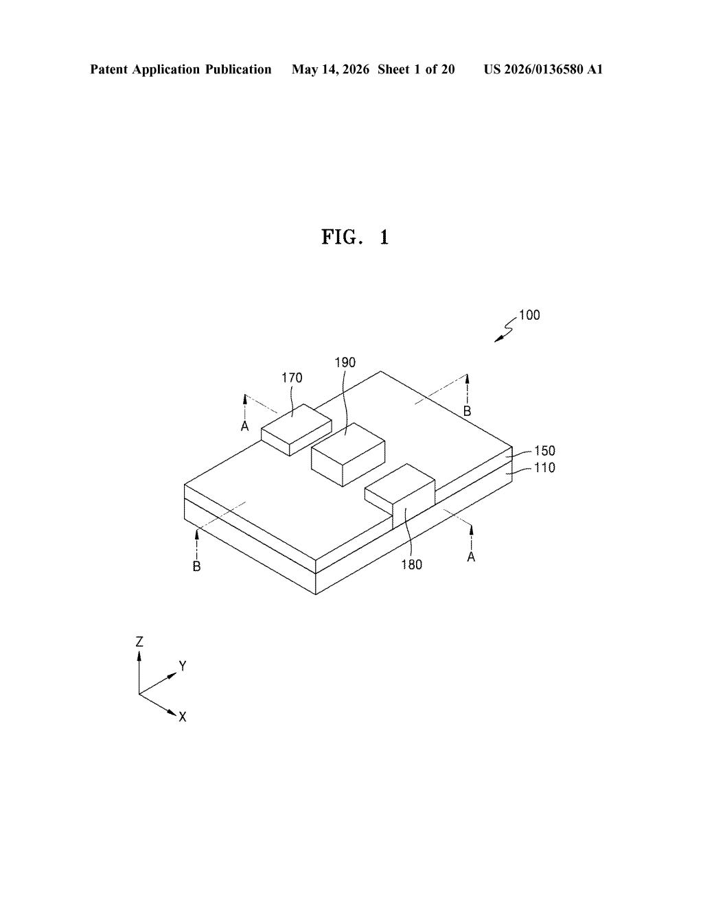
Samsung's patent describes a channel layer — the part of a transistor where electrical current flows — that's split into two zones. The active region (where current actually flows) bonds loosely to the surface beneath it, which is useful for certain electrical properties. The inactive region surrounding it bonds much more tightly, acting like a border that anchors the whole structure in place. It's a clever way to get the best of both worlds.
How active and inactive layers control adhesion in Samsung's design
The patent covers a semiconductor device built on an insulating layer, topped with a channel formation layer made from a two-dimensional (2D) semiconductor material — think materials like molybdenum disulfide (MoS₂) or tungsten diselenide (WSe₂), which are just a handful of atoms thick and have attractive electrical switching properties.
The key innovation is dividing that channel layer into two distinct lateral zones:
- Active semiconductor layer: The electrically functional region of the transistor channel. It bonds to the insulating surface below with a relatively low first adhesion energy — meaning it sits loosely, which can be desirable for preserving the material's intrinsic electronic properties.
- Inactive semiconductor layer: A border region that shares at least one chemical element with the active layer (suggesting it may be a chemically modified or oxidized version of the same material). It bonds to the same surface with a higher second adhesion energy, gripping more firmly.
The inactive layer is bonded laterally to the active layer — meaning side-by-side, not stacked on top — and its stronger grip to the substrate effectively anchors the entire channel structure. Think of it as a picture frame holding a loosely mounted print in place.
This differential adhesion approach addresses a core manufacturing challenge with 2D materials: keeping atom-thin sheets stable on surfaces without chemically disrupting the region that actually needs to conduct electricity.
What this means for ultra-thin chip and transistor development
The semiconductor industry's long-term roadmap increasingly points toward 2D materials as silicon transistors approach fundamental physical limits. But getting these ultra-thin films to stick reliably to substrates — without compromising their electrical performance — has been a stubborn materials-science problem. Samsung's approach of using a chemically differentiated border region to handle adhesion, while preserving the active channel's properties, is a practical engineering path worth watching.
For consumers, this kind of foundational work feeds into denser, faster, more power-efficient chips — the kind that would eventually show up in everything from smartphones to AI accelerators. It won't ship tomorrow, but patents like this reflect where Samsung's advanced process R&D is actually focused right now.
This is deep, unglamorous materials science — the kind of patent that rarely makes headlines but matters a lot if 2D semiconductor transistors are ever going to leave the lab. Samsung is one of only a handful of companies with the fab infrastructure to eventually commercialize this, which makes it genuinely worth noting, even if the timeline to a real product is measured in years, not months.
Get one Big Tech patent every Sunday
Plain English, intelligent commentary, no hype. Free.
Editorial commentary on a publicly published patent application. Not legal advice.