Samsung Patents a Dual-Stack Semiconductor Package With Separate Wiring Paths
Samsung has filed a patent for a semiconductor package that stacks two groups of chips on top of each other — but routes their electrical connections through entirely separate paths. It's a structural tweak, but one that matters a lot in the world of high-density chip packaging.
What Samsung's two-tier chip stack actually does
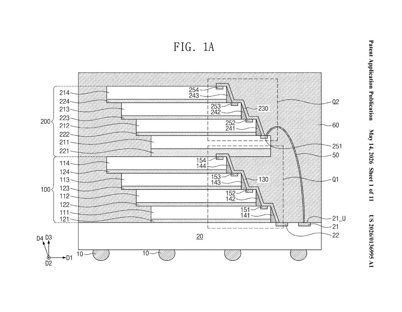
Imagine a building with two separate electrical systems — one for the ground floor and one for the upper floors — each wired independently so they don't interfere with each other. Samsung's patent describes something similar inside a chip package.
A semiconductor package is the housing that holds multiple chips together and connects them to a circuit board. Here, Samsung stacks two groups of chips — a lower stack sitting on the package substrate (the base board), and an upper stack sitting on top of that. Each group has its own wiring system, and crucially, the upper stack connects back to the base board via a thin wire bond, while the lower stack uses a different pad and connection method entirely.
The practical goal is to keep the two layers electrically independent while still fitting everything into a compact, vertically stacked package — something that's increasingly important as chips get denser and more powerful.
How the upper and lower stacks route signals differently
The patent describes a semiconductor package with three main layers: a package substrate (the base), a lower stack structure, and an upper stack structure.
The substrate has two distinct pads — first pad and second pad — that serve different stacks. The lower stack connects its chips to the second pad via a lower conductive structure, which likely refers to through-silicon vias (TSVs) or solder bumps that pass signals vertically through the stack. The upper stack connects its chips to each other via an upper conductive structure, and then reaches all the way back down to the substrate's first pad via a wire bond — a thin metal wire looped from chip to pad.
Key structural features:
- Two electrically independent routing paths for upper and lower chip groups
- Wire bonding used specifically for the upper stack's connection to the substrate
- Lower stack uses a conductive structure (likely flip-chip or TSV-based) for its substrate connection
- Both stacks share physical space vertically but remain logically separate
This separation means signal integrity for one stack doesn't depend on the other, which can simplify design and reduce crosstalk in high-density configurations.
What this means for high-density memory packaging
High-bandwidth memory (HBM) and multi-chip packages are central to AI accelerators and modern smartphones. As the number of stacked dies increases, routing signals cleanly between layers without interference becomes a real engineering challenge. Samsung's approach — giving each stack tier its own dedicated substrate pad and connection method — is a straightforward way to reduce that complexity.
For you as a consumer, this kind of packaging innovation is what allows more memory and compute to fit into the same physical footprint in your phone or laptop. It's not glamorous, but stacking architecture is quietly one of the most competitive battlegrounds in the semiconductor industry right now.
This is fairly routine semiconductor packaging IP — the kind of structural variation that Samsung files dozens of every year. There's no obvious breakthrough here, just a specific wiring topology that Samsung wants to protect. Unless you're a packaging engineer or following HBM supply chain dynamics, this one doesn't demand your attention.
Get one Big Tech patent every Sunday
Plain English, intelligent commentary, no hype. Free.
Editorial commentary on a publicly published patent application. Not legal advice.