
Xilinx Patents an On-Chip Data Bus That Confirms Message Delivery Order
When different parts of a chip send each other instructions, there's no guarantee the messages arrive in the right order. Xilinx's new patent describes a communication layer that adds explicit delivery confirmation to fix that.
What Xilinx's delivery-confirmation chip bus actually does
Imagine sending three text messages in a row and having no idea which one your friend actually read first. Inside a chip, the same problem happens constantly: one block of circuitry sends instructions to another, but there's no built-in receipt to confirm they were handled in the right sequence.
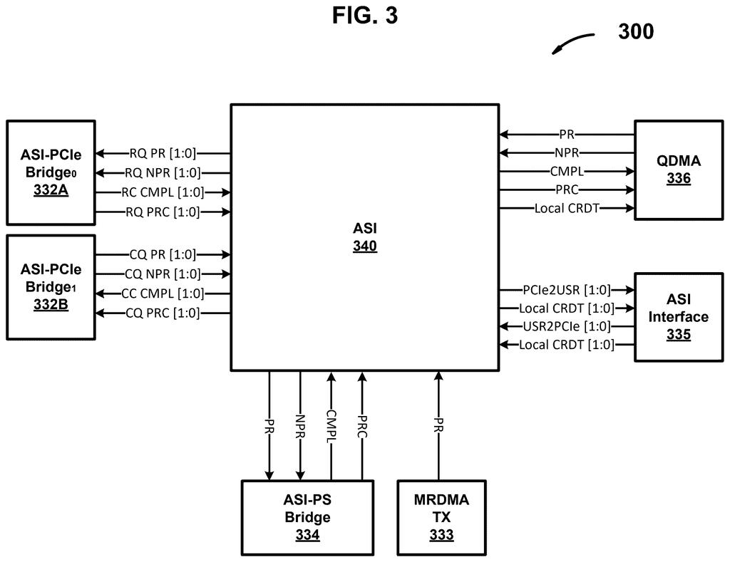
Xilinx, the programmable chip company owned by AMD, has patented a system called an Adaptable Streaming Interconnect (ASI). It acts like a courier service running inside a chip: when one component sends a request to another, the ASI ferries it across and then carries a confirmation receipt back. The sending component waits for that receipt before deciding what to do next.
This sounds simple, but enforcing message order reliably inside a complex chip is genuinely tricky. The patent describes doing it in a way that works across different types of components sharing the same internal bus, which matters for the flexible, reprogrammable chips Xilinx specializes in.
How the ASI tracks posted requests end-to-end
The patent covers a system-on-chip (SoC) architecture built around three pieces: a request initiator (the component sending work), a request target (the component doing the work), and the ASI sitting in between.
The flow works like this:
- The initiator sends a posted request (PR), a "fire and move on" style message that doesn't wait for an immediate reply.
- The ASI forwards that request to the target.
- Once the target finishes, it sends back a posted request complete (PRC), a completion signal.
- The ASI delivers that completion signal back to the initiator.
The key detail is that the initiator itself enforces ordering based on those completions. It uses the PRC receipts to decide when it's safe to issue the next request, rather than relying on a central arbiter to manage sequencing.
This is meaningful for FPGA-based SoCs (chips whose logic can be reprogrammed after manufacture), where components from different design blocks need to share a bus without one component's timing assumptions breaking another's.
What this means for programmable chip design
For chip designers building on Xilinx's programmable platforms, predictable message ordering is a persistent headache. When you're composing a chip from reusable blocks, each block may have different timing requirements, and a shared communication bus has to satisfy all of them without forcing every block to implement its own ordering logic.
This patent puts that ordering responsibility at the interconnect level, which keeps individual components simpler and makes the whole system easier to verify. It's the kind of infrastructure improvement that rarely shows up in product announcements but affects how reliably complex chips work in real deployments, particularly in data center accelerators and embedded applications where Xilinx competes most directly.
This is a foundational chip-plumbing patent, not a headline feature. It solves a real and recurring problem in SoC design, but it's the kind of work that engineers appreciate more than general readers. If you're following AMD's Xilinx roadmap for data center FPGAs, this signals ongoing investment in the low-level interconnect infrastructure that makes larger chip designs tractable.
There are more where this came from
We read every patent application Big Tech publishes and send you the ones worth knowing. Plain English, free, every week.
The drawings
13 drawing sheets from US 2026/0220340 A1 · click any drawing to enlarge


Want this weekly breakdown for a company we don't cover? Patentlyze Pro →