
Folded Laser Beam Patent Could Shrink Gadgets That Measure Distance
Apple is patenting a way to shrink a depth-sensing laser system by literally folding the beam's path inside a tiny glass block, letting a single emitter do the work of a much larger optical assembly.
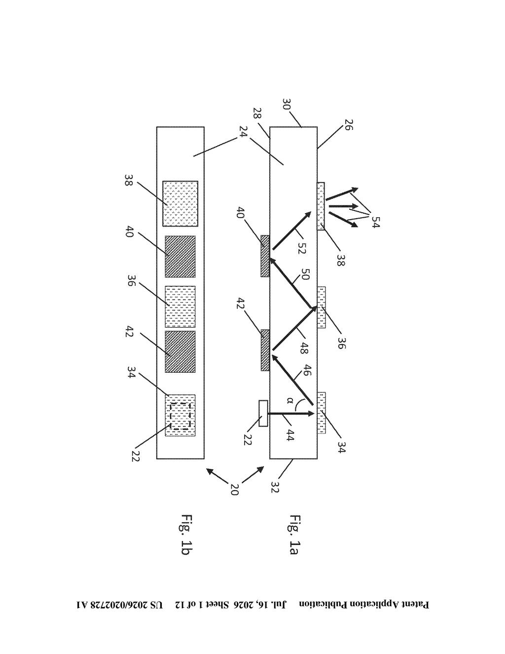
What Apple's bouncing-laser depth sensor actually does
Imagine trying to fit a ping-pong table inside a phone. That's roughly the challenge Apple faces when building depth sensors: the light beam needs to travel a meaningful distance before it can do useful work, but there's almost no room inside a device. Apple's answer, described in this patent, is to bounce the beam back and forth inside a small transparent block of glass or similar material, like a pinball in a very tight machine. The path gets folded up so the effective travel distance is long even though the physical hardware is tiny.
On the surface of that glass block sit special flat optical structures called metasurfaces (think of them as ultra-precise gratings etched at the microscopic level). These structures intercept the beam at exact points, split it into dozens of output beams, and aim each one precisely outward to project a grid of dots onto whatever is in front of the sensor. That dot pattern is what lets the device measure depth, the same basic trick used in Face ID today.
How metasurfaces split and aim the beam at the exit point
The patent describes an optoelectronic apparatus (a device that combines electronics with light) built around three core elements:
- An emitter that fires a coherent (laser-like) beam of light
- An optical substrate, which is a rectangular block of transparent dielectric material (glass or a similar insulating, see-through solid) shaped as a parallelepiped (essentially a 3D rectangle). The block is positioned to catch the beam and guide it along a path that bounces off internal walls multiple times before exiting, a technique called total internal reflection.
- Metasurfaces, flat surfaces patterned at the nanoscale, placed at specific points where the bouncing beam hits the block's faces. These surfaces split the single input beam into many output beams and collimate them (meaning they shape each one into a tight, parallel shaft of light) to project a precise pattern of dots onto a target object.
The "folded" path is the key engineering trick. By zigzagging the beam through the substrate, Apple can achieve a longer optical path, which translates to better beam shaping and splitting, without making the overall module physically larger. The metasurfaces replace bulkier conventional lenses and diffractive elements, keeping the whole assembly thin and flat.
What this means for Face ID and spatial sensing hardware
Depth sensors that project dot patterns are already inside every iPhone with Face ID, and they appear in various AR and robotics systems. The standing challenge is making them smaller and cheaper without sacrificing accuracy. A folded-path design inside a single glass substrate could let Apple shrink the sensor module further, which matters enormously when you're trying to fit more capability into a device that also needs a battery, cameras, and antenna arrays.
This kind of optical miniaturization is also relevant beyond phones. Thinner depth sensors are a prerequisite for the compact AR glasses form factor that the industry is working toward. If Apple can produce an accurate structured-light projector in a package thin enough to fit into the frame of a pair of glasses, the sensor design described here would be a plausible path to get there.
This is genuinely interesting optical engineering, not a vague software idea. Folding the beam path through a solid substrate with metasurface exits is a real miniaturization strategy, and the three-inventor team suggests focused lab work rather than a defensive filing. Whether it ends up in a phone, glasses, or something else, this is the kind of component-level patent that tends to show up in shipping hardware a few years later.
Get our take in your Top Stories
Liked this breakdown? Add Patentlyze as a preferred source on Google, and our plain-English take shows up more often in your Top Stories the next time Apple patent news breaks.
There are more where this came from
We read every patent application Big Tech publishes and send you the ones worth knowing. Plain English, free, every week.
Want this weekly breakdown for a company we don't cover? Patentlyze Pro →