
Google Patents a Dedicated Chip Component to Speed Up AI Math Calculations
Google is patenting a small but specialized piece of chip architecture whose only job is to figure out which part of a processor handles which slice of an AI calculation, so nothing waits around for instructions that are stuck in the wrong place.
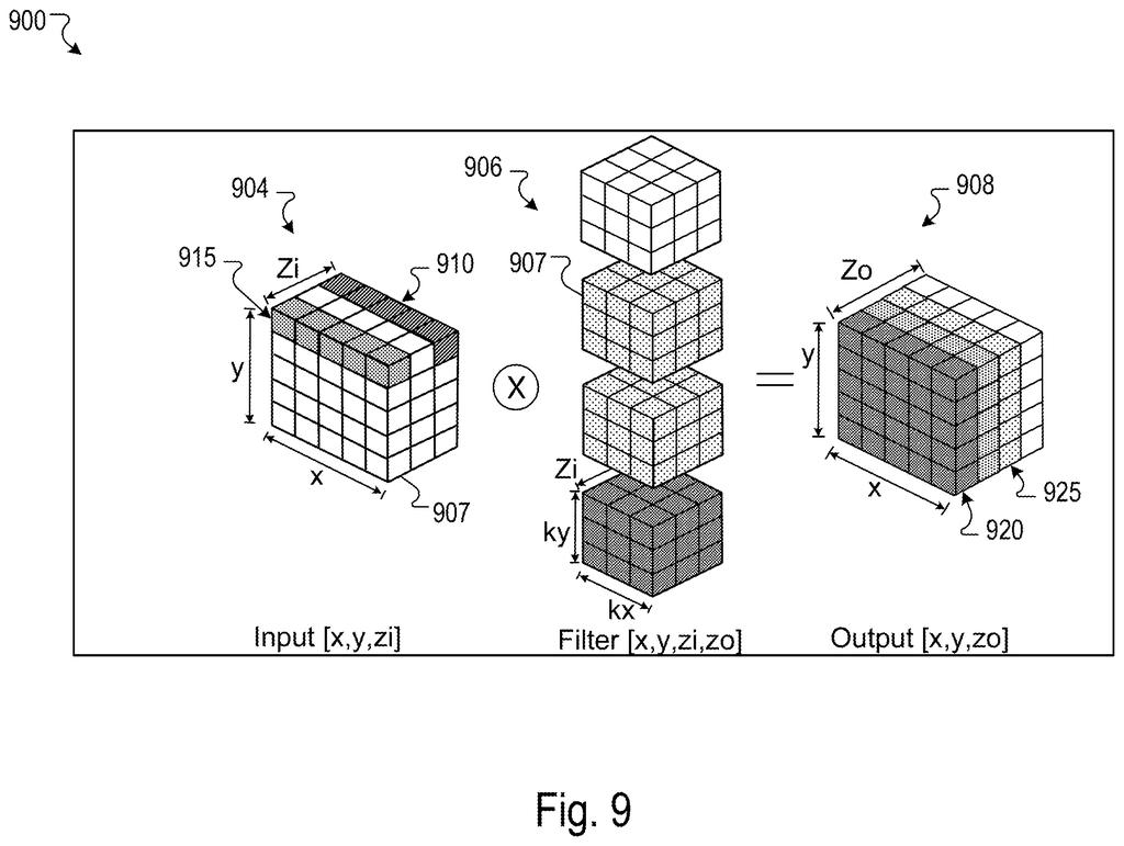
What Google's tensor mapping unit actually does inside a chip
Every time a Google data center runs an AI model, thousands of individual math operations have to get sorted and sent to the right part of a processor chip. That sorting step sounds simple, but at the speeds modern AI chips run, even a small delay in routing work to the right spot wastes real time and real energy.
Google's new patent describes a dedicated unit baked directly into the chip whose only job is that routing work. Instead of making the main processor figure out where each piece of a calculation lives, this unit reads an instruction, maps out exactly which positions in a data array belong to which slice of the chip, and fires off the precise signals needed to fetch those numbers from the right local memory. The main processor never has to stop and sort things out itself.
The practical effect is that AI math, particularly the kind of large matrix operations that power tools like Google's own language models, can move through the chip with less overhead and fewer stalls.
An integrated circuit configured to accelerate tensor computations for a machine-learning model implemented at the integrated circuit, the integrated circuit comprising: a processing engine; and a tensor mapping unit configured to: generate a plurality of tensor element positions for a tensor based on an instruction received from the processing engine …
Translation: The chip includes a specialized unit that calculates exactly where data should go to speed up artificial intelligence tasks.
How the mapping unit assigns tensor positions to compute tiles
The patent covers a chip component called a tensor mapping unit (TMU). A tensor, in this context, is just a structured grid of numbers, the same kind of data structure that AI models constantly multiply, add, and transform. Chips built for AI work tend to break those grids into chunks and farm the chunks out to many small processor sections called compute tiles, each with its own local memory.
The problem the TMU solves is coordination. When the main processing engine issues an instruction, something has to determine which tile owns which chunk of the tensor and then fetch the right numbers from that tile's memory. Today that bookkeeping can sit with the central processor, adding overhead. The TMU offloads it entirely.
- Position generation: The TMU reads the incoming instruction and works out the full list of element positions inside the tensor (think: row and column addresses in the data grid).
- Tile assignment: It checks which positions belong to which compute tile on the chip.
- Control signal dispatch: It sends precise fetch commands directly to the correct tile memory, bypassing the central processor for that work.
The result is a tighter pipeline: each compute tile gets its inputs faster because the routing decision is made by dedicated hardware rather than shared processing resources. The patent frames this as an acceleration mechanism specifically for machine-learning models running on custom integrated circuits, which points squarely at Google's in-house Tensor Processing Unit (TPU) line.
… determine that a first subset of the tensor element positions is assigned to a first compute tile of the integrated circuit; and iii) generate control signals to obtain a group of inputs from a tile memory of the first compute tile based on the first subset.
Translation: The system identifies which specific part of the chip should handle a piece of data and then pulls that data from memory.
What this means for Google's custom AI chip strategy
Google designs its own AI chips, the TPU family, specifically to run the matrix math that neural networks demand. Any architecture that reduces the cycles the main processor spends on bookkeeping means more of the chip's budget goes toward actual computation. For data centers running AI inference at scale, that kind of efficiency compounds quickly across millions of requests.
The TMU concept is also a signal about how Google thinks about chip specialization: offload every repeatable coordination task to a fixed-function unit so the programmable cores stay free. That philosophy has driven the TPU roadmap for years, and this patent extends it one level deeper into the memory-fetch pipeline. Coverage of new Big Tech patents in the AI chip space shows this kind of fine-grained memory-routing work is where the real architectural competition is happening right now, well below the level of headline transistor counts.
The design trade here is legibility for speed: by handing routing decisions to a fixed-function unit, Google locks in assumptions about how tensors are partitioned across tiles. That works beautifully when the workload fits the expected pattern and breaks down when a model uses irregular tensor shapes or sparse data that doesn't tile cleanly. The TMU approach bets that AI workloads are regular enough that the inflexibility cost is low, and for Google's own models running on Google's own chips, that bet is probably well-placed. The real risk shows up at the edges, when third-party models or unusual architectures hit hardware that was optimized around a different assumption.
There are more where this came from
We read every patent application Big Tech publishes and send you the ones worth knowing. Plain English, free, every week.
The drawings
9 drawing sheets from US 2026/0236732 A1 · click any drawing to enlarge


Want this weekly breakdown for a company we don't cover? Patentlyze Pro →
Be the first to weigh in