Google Patents a Side Sideband Interface for Flexible Die-to-Die Chip Communication
As chips get built from multiple smaller dies stacked or tiled together, getting those dies to talk to each other reliably — and cheaply — is one of the unsexy but critical engineering problems of modern silicon design. Google's latest patent takes a direct swing at it.
What Google's Side Sideband Interface actually does
Imagine a modern chip that's actually several smaller chips glued together in one package — like assembling a puzzle instead of carving one big piece. Each piece (called a die) needs to send messages to the others constantly. The wiring that handles those messages needs to be fast, reliable, and not too power-hungry.
Google's patent describes a new kind of internal interface called the Side Sideband Interface (SSBI). Think of it as a smart post office inside a chip package: it accepts letters written in many different formats, converts them all into one standard format, routes them to the right destination, and makes sure nothing gets lost or jammed in transit.
The key trick is that the SSBI doesn't force every part of the chip to speak the same language upfront. It handles translation and traffic control in the middle, which means you can mix different chip components without redesigning everything from scratch. That makes building complex multi-die chips cheaper and more flexible.
How the SSBI serializes, arbitrates, and controls flow
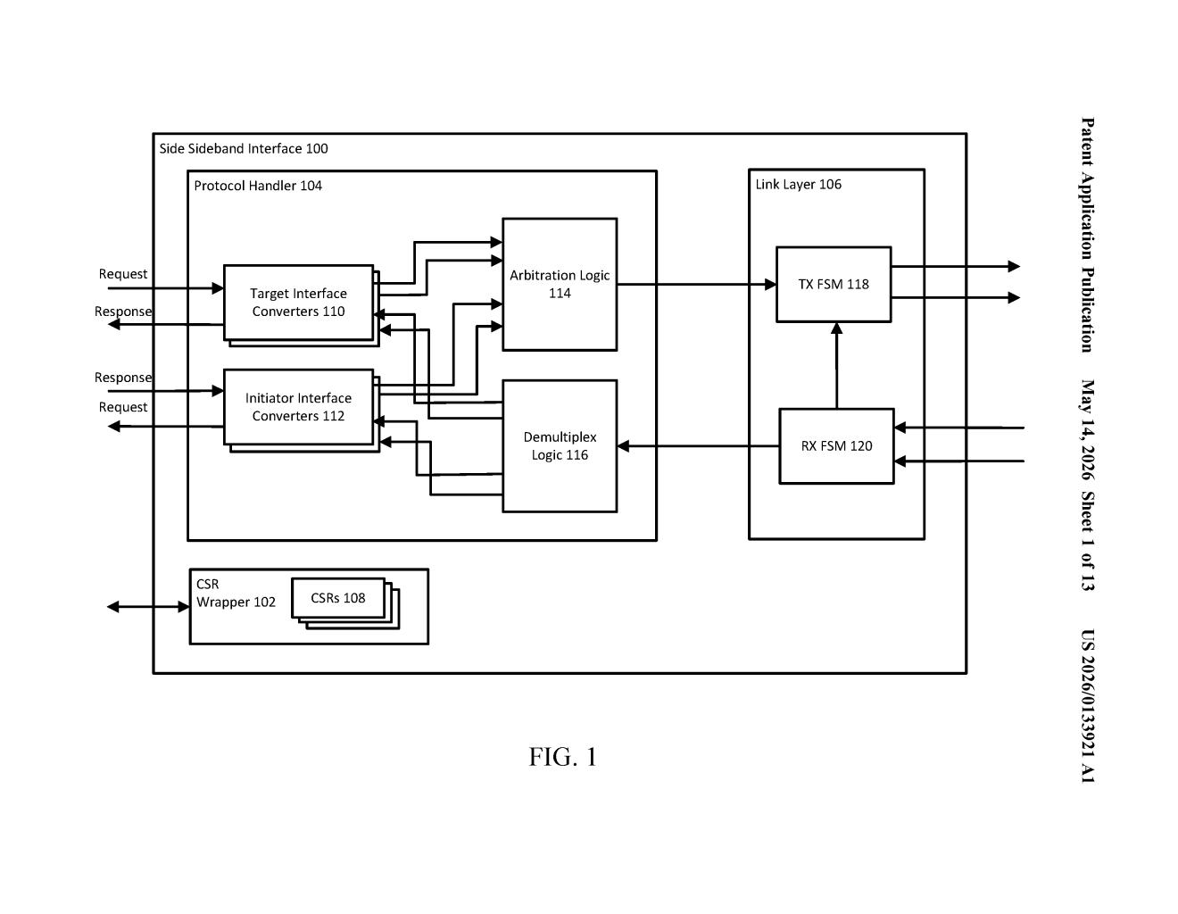
The SSBI sits between different dies in a multi-chip package and handles communication through three main components:
- CSR Wrapper — a set of configuration and status registers (think: settings and diagnostics dials) that let software configure and monitor the interface without needing custom hardware hooks.
- Protocol Handler — converts multiple incoming protocols (different 'languages' that different chip blocks speak) into a single standard streaming interface, then performs arbitration (deciding whose message goes first when multiple senders compete) and demultiplexing (sorting incoming traffic back out to the right destination).
- Link Layer — uses a set of finite state machines (FSMs) — essentially step-by-step decision logic circuits — to serialize outgoing data (breaking it into a stream of bits for the physical wire), deserialize incoming data (reassembling those bits), manage credit-based flow control (a traffic-throttling system where senders only transmit when the receiver has confirmed it has buffer space), and detect errors.
The credit-based flow control is worth highlighting: rather than letting a fast sender overwhelm a slower receiver and drop data, the system hands out 'credits' — permissions to send — so the link self-regulates without needing retransmissions. That's a well-established technique in high-speed interconnects (PCIe uses it too), but applying it inside a die-to-die sideband interface adds robustness at relatively low hardware cost.
What this means for Google's multi-die chip strategy
Multi-die chip packaging — often called chiplet architecture — is now mainstream across the industry. AMD, Intel, Apple, and Nvidia all ship chiplet-based products. Google's TPUs and custom silicon (used in data centers and Pixel devices) are increasingly complex, and managing the sideband communication between dies is a real engineering cost center.
A flexible, protocol-agnostic sideband interface like the SSBI could let Google's chip teams reuse the same interface IP across different projects without custom glue logic each time. That translates directly into faster tape-outs and lower engineering costs. For you as a user, chiplet efficiency ultimately affects how much compute Google can pack into a device or a data center rack at a given power budget.
This is solid, unglamorous chip plumbing — the kind of patent that matters a lot to chip architects and almost nobody else. It's not a moonshot idea; credit-based flow control and protocol normalization are established techniques. What's notable is that Google is systematically building and patenting its own die-to-die interconnect IP rather than relying entirely on industry standards like UCIe. That's a real signal about how seriously Google is investing in custom silicon infrastructure.
Which company should we read for you?
We track 17 companies here. Pro is the same weekly breakdown for any company you choose, delivered privately. Type a name and we'll scope it and send you a quote.
Get one Big Tech patent every Sunday
Plain English, intelligent commentary, no hype. Free.
Editorial commentary on a publicly published patent application. Not legal advice.