
IBM Patents a Two-Layer Chip Surface to Keep Medical Sensors Reading Accurately
Medical sensor chips tend to lose their grip: the molecules that catch the target can peel off in liquid and skew the reading. IBM's patent application adds stacked layers underneath to hold them on.
What IBM's two-layer biosensor chip actually does
Ever had a sticker peel off a water bottle after a few weeks of washing? Tiny medical sensor chips have a similar headache.
Many of these diagnostic chips work by coating a surface with molecules that grab onto a target, such as a virus or a protein. Put the chip in liquid, and that coating can slowly come loose. The reading then drifts even when nothing in the sample has changed.
IBM's patent application goes after the problem from underneath. Instead of a single layer beneath the coating, the chip gets two or more thin stacked layers of metal oxide or metal nitride, and the coating is attached to the top one. In IBM's own tests, the stacked version produced a much more stable signal over time.
… a gate electrode that modulates current through the semiconductor channel, the gate electrode comprising two or more stacked layers, wherein the two or more stacked layers are composed of an oxide or a nitride; and a biorecognition layer grafted to a top surface of the gate electrode.
Translation: The sensor uses a layered metal surface topped with biological material to detect specific medical targets.
How the stacked coating keeps molecules attached
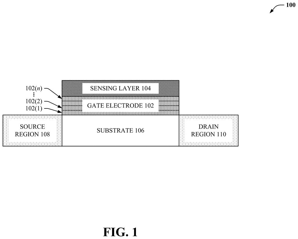
The device is a biosensor built like a transistor. A gate electrode (the conductive part that controls how much current flows through the chip's channel) sits under a sensing coating called the biorecognition layer. When a target molecule sticks to that coating, the surface charge shifts, the current changes, and the chip reports a measurable signal.
The filing says existing chips use a single conductive layer here, and the coating often detaches during measurement. The cause is hydrolysis (water breaking the chemical bonds that anchor the coating). Detachment weakens the signal, hurts the lowest amount the chip can detect, and makes readings wander.
IBM's fix is a gate electrode made of two or more stacked layers, each an oxide or a nitride. In the main example, a base of hafnium dioxide or titanium nitride (about 4 nanometers) is topped with zirconium dioxide (about 1.5 nanometers). The coating is then chemically attached to that top layer:
- Clean the base layer and grow the zirconium dioxide layer from a solution.
- Add a phosphonic acid chemical that organizes itself into a one-molecule-thick coating.
- Optionally attach a biotin-based sensing molecule through a linker.
In tests on nine sample devices plus a control, the signal stayed stable over time. Single-layer devices showed large swings. The filing also describes bipolar junction transistor and optical versions of the same idea.
One or more systems, devices and/or methods of fabrication provided herein relate to forming a semiconductor device for biosensing with enhanced temporal stability.
Translation: This invention creates a medical sensor that stays accurate over a long period of time.
Why steadier sensors matter for quick medical tests
Quick tests done at or near the patient, with no lab needed, only help if you can trust the number on the screen. A sensor whose coating slowly peels off gives readings that wander, which is a problem for any test that has to run for a long time. Keeping that coating attached is a basic step toward readings people can rely on.
The filing treats this as a materials fix rather than a new sensor design. A silicon wafer can already carry an oxide or nitride film that serves as the first layer, so the extra layer is a small addition to the structure. The filing names no product and shows results from sample devices, so this is early-stage chip engineering.
IBM's 22nd chip filing we've tracked since May joins others like one on catching stray light and one on joint bug hunting in our chip patent coverage.
Claim 1 covers any sensor chip that combines three things: a semiconductor channel, a gate electrode built from two or more stacked layers of oxide or nitride material, and a biological recognition layer attached to the top. No specific disease target, molecule, or readout method is required. Any chip assembled that way falls inside it.
That scope is wide. A manufacturer building sensors for cancer markers, waterborne pathogens, or agricultural toxins using this layered gate structure would need IBM's permission, because the claim draws its boundary at the structural idea of stacking, not at any particular application or material choice.
What this blocks in practice is a generation of biosensor hardware built around the layered gate approach, regardless of what the sensor is hunting for or how it reports results. Since construction is where manufacturing decisions actually live, this claim reaches the decisions that matter most.
Get our take in your Top Stories
Liked this breakdown? Add Patentlyze as a preferred source on Google, and our plain-English take shows up more often in your Top Stories the next time IBM patent news breaks.
There are more where this came from
We read every patent application Big Tech publishes and send you the ones worth knowing. Plain English, free, every week.
The drawings
14 drawing sheets from US 2026/0309672 A1 · click any drawing to enlarge


Want this weekly breakdown for a company we don't cover? Patentlyze Pro →
Be the first to weigh in