IBM Patents a Shared-Register System for Diagnosing Failing On-Chip Memory
When memory cells on a chip start failing, knowing exactly which ones and how many are broken is half the battle. IBM's new patent describes a tidy three-register bookkeeping system that keeps track of those failures — and flags when the damage is too widespread to repair.
How IBM tracks broken memory cells on a single chip
Imagine a chip crammed with dozens of small memory arrays, each storing bits of data. Over time — or even right off the factory line — individual columns inside those arrays can fail. The hard part isn't detecting one bad column; it's knowing how many arrays are broken and whether the chip is still salvageable.
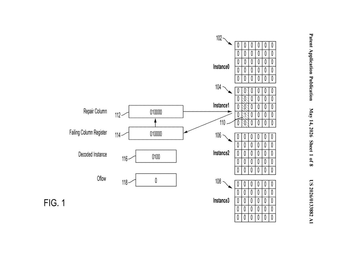
IBM's patent describes a set of three shared registers — think of them as tiny scoreboards etched onto the chip itself. The first scoreboard notes which columns are failing. The second notes which memory arrays have problems. The third, crucially, raises a flag the moment more than one array is failing at the same time.
That overflow flag is the key insight. A single bad array can often be repaired using redundant circuitry built into the chip. But when multiple arrays fail together, repair gets complicated fast — and the chip may need to be discarded. This system tells test equipment exactly when that threshold is crossed.
How the three-register chain flags and counts failures
The patent covers a chip-level diagnostic architecture built around three cooperating registers that collectively describe the failure state of all on-chip memory arrays.
- First register (column latch): Shared across all memory arrays. It receives failing column status data — essentially a signal saying "this column inside this array has a bad cell" — and stores a status bit for it.
- Second register (array status register): Receives failing memory array status data and sets a bit identifying which array or arrays are in trouble.
- Third register (overflow register): Coupled to the second register and sets an overflow status bit when more than one memory array is simultaneously flagged as failing.
The overflow bit is what separates diagnosable-and-repairable faults from situations where repair logic would be overwhelmed. Because repair resources (like redundant rows and columns) are finite, a chip with two or more concurrently failing arrays may exceed what the built-in repair circuitry can handle.
This architecture allows test equipment and on-chip repair logic to make a fast, deterministic decision: apply repair to the flagged instance, or mark the chip as unrecoverable. The claim is deliberately hardware-level — these are physical registers on the die, not software counters.
What this means for chip yield and post-silicon repair
For IBM, which designs dense mainframe and server chips where memory array count is high and yield is critical, having a reliable way to triage failures at test time directly affects manufacturing economics. A chip that can be repaired in place is worth far more than one that gets scrapped.
More broadly, as chip designs pack more memory arrays onto a single die — think high-bandwidth memory controllers, AI accelerators, or processor last-level caches — the likelihood of at least one array failing goes up. A clean, shared diagnostic register structure like this one is the kind of unglamorous infrastructure that makes large-scale chip testing faster and more decisive. You won't see this feature marketed on a spec sheet, but it quietly affects how many chips make it out of the fab.
This is a workmanlike chip-design patent — not flashy, but genuinely useful. The overflow register concept is the one clever idea here: it converts a messy multi-array failure state into a single binary flag that downstream repair logic can act on instantly. That's good engineering. IBM files a lot of memory diagnostics patents, and this one fits neatly into that portfolio.
Get one Big Tech patent every Sunday
Plain English, intelligent commentary, no hype. Free.
Editorial commentary on a publicly published patent application. Not legal advice.