
Qualcomm Patents a Graphics Chip That Checks Its Own Active Sections Before Dividing Work
Qualcomm's latest patent describes a GPU that looks up a simple on/off list of its own active sections before handing out graphics work, which sounds obvious until you realize most GPUs don't handle partial configurations this cleanly.
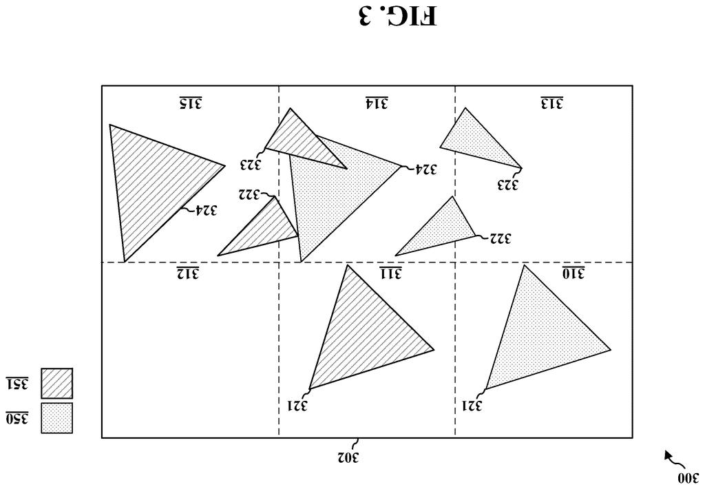
What Qualcomm's slice-mask GPU actually does
Imagine a restaurant kitchen where some stations are closed for the night. A good manager checks which stations are open before assigning orders, rather than sending tickets to stations that can't respond. Qualcomm's patent describes a GPU that does exactly this kind of check before it starts drawing anything on your screen.
Every GPU is made up of smaller working sections. This patent lets the chip read a quick lookup table, called a slice mask, that records exactly which sections are switched on and available. The GPU then hands out two types of graphics work, calculating the shape of objects and filling in their colors, only to the sections that are actually running.
The practical upside is that the same chip design can work with four active sections or sixteen, without needing different software for each configuration. That flexibility matters a lot when Qualcomm wants to sell the same GPU core across phones, tablets, and laptops at very different price points.
obtain, from a register of a graphics processor, a slice mask for a set of slices available to the graphics processor; distribute a set of vertex shading tasks to the set of slices based on the obtained slice mask; and distribute a set of pixel shading tasks to the set of slices based on the obtained slice mask.
Translation: The chip checks which parts are active and divides both vertex and pixel work accordingly.
How the slice mask routes vertex and pixel tasks
The patent centers on a slice mask, which is a compact value stored in a hardware register (a tiny, fast memory location built directly into the processor). Each bit in this mask corresponds to one slice, a self-contained processing unit inside the GPU. A 1 means that slice is active; a 0 means it's off, either because the chip was manufactured with fewer slices or because power management has disabled some.
When the GPU receives a graphics workload, it reads this mask first and uses it to direct two categories of tasks:
- Vertex shading tasks: calculations that define the 3D positions and shapes of objects in a scene
- Pixel shading tasks: calculations that determine the final color and texture of each pixel on screen
By routing both task types through the same mask, the GPU avoids sending work to slices that don't exist or aren't powered on. The design is specifically aimed at scalable GPU families, where one chip architecture ships in many product tiers. Instead of writing separate scheduling logic for each variant, the hardware reads one register and adapts automatically.
This is an infrastructure-level patent rather than a visual-output patent. The user never sees the mask; they just get a chip that doesn't waste cycles trying to use hardware that isn't there.
A graphics processor may obtain, from a register of the graphics processor, a slice mask for a set of slices available to the graphics processor.
Translation: The GPU reads its own hardware status to see which sections are currently up and running.
What this means for Qualcomm's chip scaling strategy
Qualcomm sells Snapdragon chips across an enormous range of devices, from budget Android phones to flagship laptops. Keeping one GPU architecture coherent across all those tiers is an engineering headache, because the number of active processing sections varies widely. A cleaner mechanism for telling the GPU which sections to use at runtime means Qualcomm can spin up new product variants faster and with less custom driver work per SKU.
For you as a user, the direct effect is modest but real. Chips that handle partial configurations gracefully tend to be more power-efficient and more stable when sections are disabled for thermal or cost reasons. It's the kind of plumbing change that shows up as slightly better battery life or fewer driver glitches rather than anything you'd notice on a spec sheet.
This is unglamorous but solid chip-architecture work. The slice mask idea is elegant in its simplicity, and the fact that it covers both vertex and pixel scheduling in one mechanism is the kind of detail that saves Qualcomm's driver teams real time across a wide product line. For anyone tracking how Qualcomm plans to keep Adreno GPUs competitive across tiers, but it's not a headline feature.
There are more where this came from
We read every patent application Big Tech publishes and send you the ones worth knowing. Plain English, free, every week.
The drawings
10 drawing sheets from US 2026/0228965 A1 · click any drawing to enlarge


Want this weekly breakdown for a company we don't cover? Patentlyze Pro →
Be the first to weigh in