
Samsung Patents Technology That Fixes How Memory Chips Receive Data Signals Individually
Every wire carrying data between a processor and memory chips can drift slightly out of sync, and at high speeds that drift causes read errors. Samsung's new patent describes a controller that corrects each wire's timing individually rather than applying one blunt fix to all of them.
What Samsung's per-pin memory timing fix actually does
Modern devices pack multiple memory chips side by side, and every electrical connection between those chips and the processor has its own tiny timing imperfection. Today's controllers often treat those connections as a group, applying a single timing correction that is a compromise for all of them.
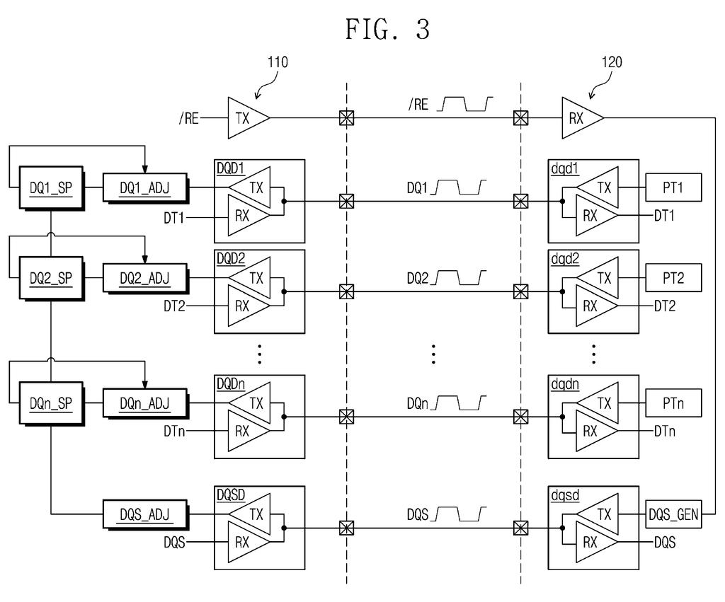
Samsung's patent describes a controller that watches each data line on its own. It runs two separate tuning routines per line: one that locks the signal to the correct moment in time, and a second that makes sure the high-and-low pulse shape is even. Both adjustments are calibrated against a dedicated timing reference signal called a data strobe.
The result is that each pin carries a cleaner, more precisely timed signal. For you as a user, that translates to more reliable memory reads, especially inside the dense, fast memory stacks found in phones, tablets, and data-center chips.
… performing a first per-pin delay locked loop (ppDLL) operation on the first reception signal and a second ppDLL operation on the second reception signal based on the data strobe signal to generate a first DLL code and a second DLL code, respectively …
Translation: The system individually adjusts the timing for each connection pin using a reference clock signal.
How the controller calibrates each data pin independently
The controller communicates with several memory chips at once and receives data through multiple signal pins simultaneously. Two calibration techniques are applied to each pin separately.
Per-pin delay locked loop (ppDLL) (a circuit that synchronizes when a signal is sampled) is run independently for each pin, producing a unique delay code per pin rather than one shared code. This corrects for the fact that different wires on a circuit board carry signals that arrive at slightly different times.
Per-pin duty cycle correction (ppDCC) then addresses a second problem: the pulse on each wire may spend unequal time in its high versus low state, which is called duty cycle distortion. The correction code for each pin ensures the rising and falling edges of its data signal line up precisely with the corresponding edges of the data strobe, the timing reference signal the memory chip sends alongside its data.
Once both codes are generated for a given pin, they are applied to all incoming data signals on that pin from across the entire group of memory chips. So a single calibration pass covers every chip connected to that pin, making the approach efficient even in systems with many memory devices wired in parallel.
… generating first and second correction signals by performing first and second per-pin duty cycle correction (ppDCC) operations on the first and second delay signals based on a falling edge of the data strobe signal, respectively …
Translation: It then fine tunes the signal pulses individually to keep the data flowing without errors.
What this means for high-speed memory in Samsung devices
Memory bandwidth is one of the tightest bottlenecks in high-end chips, from smartphone processors to AI accelerators. When timing errors creep in at high data rates, the controller has to slow down or retry reads, eating into the speed advantage that fast memory is supposed to provide. Per-pin calibration removes a source of those errors at the hardware level.
Samsung's string of memory-controller filings fits a pattern of protecting the low-level engineering that ties its DRAM and NAND products to its Exynos and custom chip business. If granted, a patent at this level of the memory interface could matter in negotiations with any chipmaker that builds controllers to talk to Samsung memory.
Samsung's 52nd filing we've tracked in the AI chip wars since June adds to a run that includes one on idle-time power cuts and one on dedicated AI data storage.
Claim 1 is written at a usefully specific level: it covers the combination of per-pin DLL and per-pin DCC, both keyed to the same data strobe signal, with the resulting codes then applied across multiple memory devices on those pins. That pairing is the heart of what this filing protects.
The practical scope is real but not sweeping. A controller that runs either technique without the other, or that uses a different timing reference, would sit outside the claim. So this is protection for a specific calibration architecture, not a general claim over all per-pin memory tuning.
For Samsung's own chip division, the filing makes sense: as memory speeds climb (LPDDR6 is already in the market), per-pin correction becomes less optional and more mandatory. Securing the specific two-step approach described here gives Samsung something concrete to point to if a licensing dispute arises over next-generation memory controller designs.
There are more where this came from
We read every patent application Big Tech publishes and send you the ones worth knowing. Plain English, free, every week.
The drawings
25 drawing sheets from US 2026/0279419 A1 · click any drawing to enlarge


Want this weekly breakdown for a company we don't cover? Patentlyze Pro →