
Samsung Patents Tiny Signal Tunnels Inside Chips That Cut Wireless Interference
Samsung wants to guide radio-frequency signals between chips using the same tiny solder bumps already holding those chips together, turning a structural component into a built-in antenna channel.
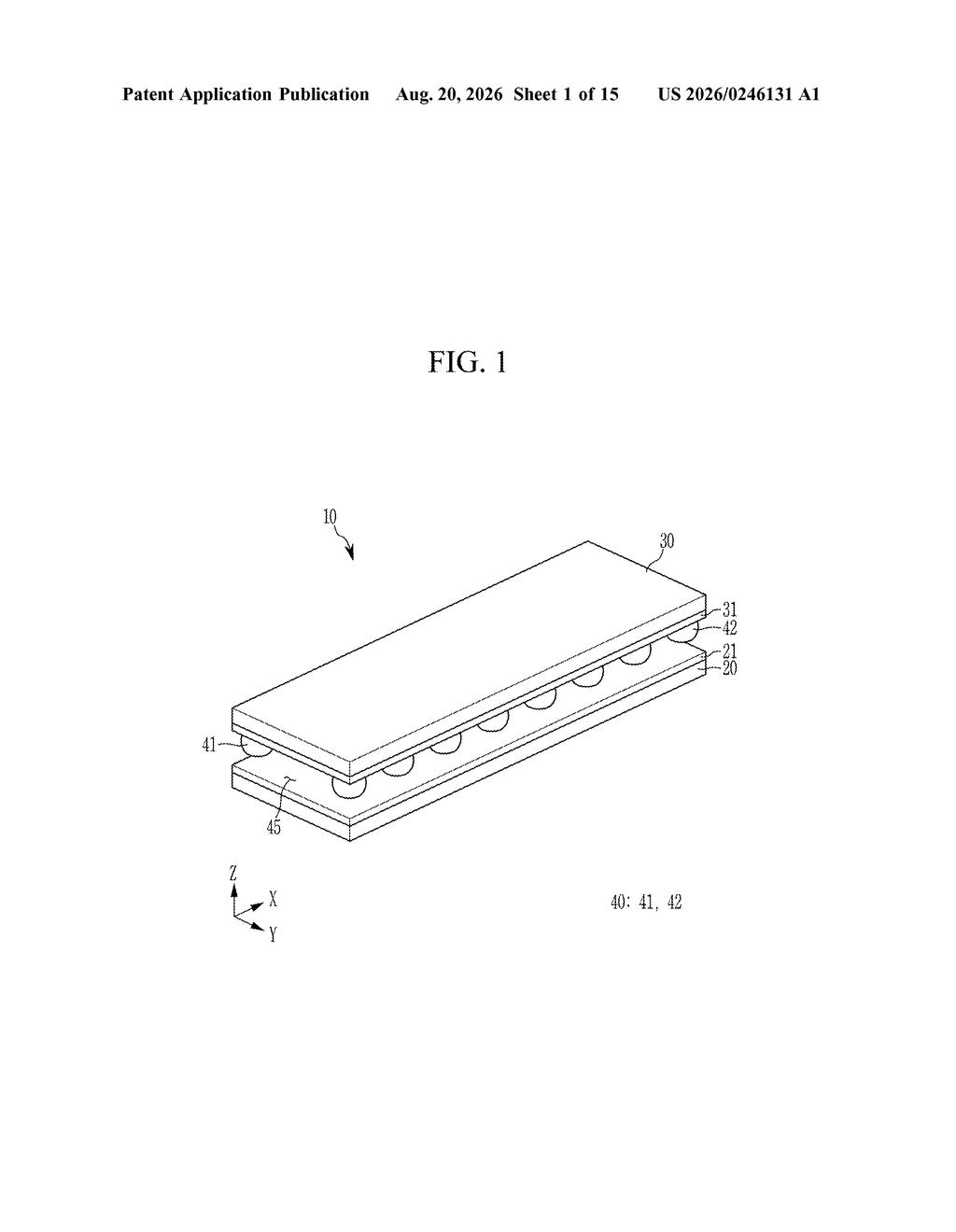
What Samsung's solder-built signal channel actually does
Every time your phone streams video or runs an AI task, chips inside it are passing enormous amounts of data to each other at very high speeds. The faster those signals travel, and the less energy they lose along the way, the better everything works.
Samsung's patent describes a way to route high-frequency signals between chips using rows of solder bumps, the small metallic dots that physically connect chips in a package. By arranging those bumps in a specific pattern, Samsung creates a channel called a waveguide that keeps radio-frequency signals contained and directed, rather than letting them scatter and lose strength.
The practical idea is that you don't need a separate dedicated component to guide those signals. The solder that's already there does double duty, which could mean less complexity and potentially better signal quality inside the tiny stack of chips in your devices.
… a plurality of solder patterns between the first wiring and the second wiring, the plurality of solder patterns spaced apart from each other in a first direction, and defining a waveguide region between the first wiring and the second wiring …
Translation: Tiny dots of solder act as walls to build a tunnel for signals.
How solder bumps define the waveguide region
The patent describes a waveguide structure built into a semiconductor package using components that already exist in standard chip assembly.
A waveguide (think of it as a controlled pipe for electromagnetic signals) is defined by:
- A first wiring layer sitting on a substrate (the base layer of the chip package)
- A second wiring layer positioned above it and facing it
- A row of solder patterns (the bumps or pads) placed between those two wiring layers, spaced evenly along one direction
The two facing wiring layers act like walls, and the spaced solder patterns act like fence posts, together enclosing a waveguide region, a defined corridor through which radio-frequency (RF) signals travel with less loss and less interference from the surrounding package materials.
The key claim is structural: the geometry of those solder patterns, their spacing and positioning between the two opposing wirings, is what creates the waveguide channel. No exotic new material is required. The same solder used to bond chip layers mechanically is shaped and arranged to also function as an RF guide.
… a waveguide region extending along the first direction between the first wiring and the second wiring.
Translation: A channel that guides wireless signals safely through the chip.
What this means for high-speed chip packaging
As chips are stacked closer together in advanced packages (a trend driven by AI accelerators, 5G modems, and memory-on-logic designs), moving high-frequency signals between those layers without loss or interference becomes one of the harder engineering problems. Separate waveguide components add cost and physical space that dense packages don't have.
If solder patterns can serve as both a mechanical bond and a signal channel, that's one fewer discrete component in a very crowded space. Samsung is one of the largest makers of advanced chip packages in the world, and this approach fits directly into its HBM memory and advanced packaging roadmap. The broader push to integrate RF signal routing into package structures is one of the more active areas among new Big Tech patents in semiconductor packaging.
Samsung's 39th filing we've tracked since June in the AI chip wars follows one on translating memory requests and one on stopping screen stutter.
When chips are stacked on top of each other, high-speed signals bleed away before they arrive. That waste gets worse as speeds rise, and it costs money. Samsung's fix routes those signals through a path shaped by the solder bumps already holding the chips together, so no new parts are needed.
The fix is narrow in what it tackles. But a narrow fix aimed at a real, expensive problem still makes dense, fast chip stacks work better in actual products.
Get our take in your Top Stories
Liked this breakdown? Add Patentlyze as a preferred source on Google, and our plain-English take shows up more often in your Top Stories the next time Samsung patent news breaks.
There are more where this came from
We read every patent application Big Tech publishes and send you the ones worth knowing. Plain English, free, every week.
The drawings
15 drawing sheets from US 2026/0246131 A1 · click any drawing to enlarge


Want this weekly breakdown for a company we don't cover? Patentlyze Pro →
Be the first to weigh in