
Samsung Patents Screen Layers That Produce Sharper, Truer Colors in Headset Displays
Getting accurate, vivid color out of a display small enough to sit in a pair of glasses is one of the hardest problems in AR hardware. Samsung's latest patent targets that problem by stacking two different color-converting materials inside each individual pixel.
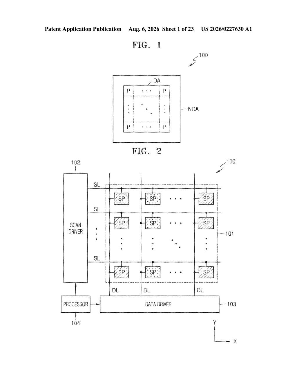
What Samsung's two-layer pixel color trick actually does
Imagine each pixel in a display as a tiny well. The light source at the bottom emits one color (usually blue or ultraviolet), and a special material lining the well converts that light into the red, green, or blue your eye is supposed to see. The quality of that conversion determines how accurate and bright the final image looks.
Samsung's patent describes a way to build those pixel wells with two stacked layers of color-converting material instead of one. Think of it like a two-stage filter: the first layer does an initial conversion, and the second layer (made of a different material) refines the result. Tiny walls etched directly from the light-emitting structure separate each pixel so colors don't bleed into their neighbors.
The manufacturing process is notable too. Samsung carves the pixel walls out of the same semiconductor material that generates the light, rather than building them separately. That tight integration is the kind of precision engineering you need when you're trying to pack millions of pixels into a display that fits inside a pair of glasses.
… forming a plurality of first color conversion layers in a plurality of opening areas between the plurality of partition walls; and forming a plurality of second color conversion layers on the plurality of first color conversion layers …
Translation: The manufacturing process layers two different materials to help tune and improve the display colors.
How the partition walls and stacked layers are built
The patent covers both the physical structure of the display and the step-by-step process for making it.
At the heart of the design are micro-LED light emitting elements, each built from a sandwich of semiconductor layers with an active layer (the part that actually produces light) in the middle. After the semiconductor stack is grown on a temporary substrate, that substrate is removed, exposing a flat surface of the top semiconductor layer.
From that exposed surface, Samsung etches away material to form partition walls that physically separate each pixel's color-conversion zone. Because the walls are carved from the same semiconductor, they are extremely thin and precise. The process also ensures that each active layer (the light source) faces directly into its own color-conversion opening, minimizing light waste.
Inside each opening, two color conversion layers are deposited in sequence:
- First color conversion layer: an initial material that begins shifting the LED's native wavelength toward the target color.
- Second color conversion layer: a different material stacked on top that completes or refines the conversion.
Using two chemically distinct materials gives Samsung more control over the final color output and efficiency than a single-layer approach would allow.
… a plurality of color conversion layers provided on the plurality of light emitting elements in correspondence with the plurality of light emitting elements and spaced apart from each other by the plurality of partition walls …
Translation: Small physical walls separate the color filters to keep the light clean and distinct for each pixel.
What this means for future Samsung AR glasses
For augmented reality displays, pixel density and color accuracy are everything. A display that bleeds color between pixels, or that wastes light during conversion, produces a dim or muddy image. Samsung's stacked conversion approach and integrated partition walls directly address both of those failure modes at a manufacturing level.
This filing signals that Samsung is investing in the low-level display fabrication work needed to make AR glasses with genuinely good image quality. The technique is compatible with the micro-LED pixel sizes that next-generation AR headsets and glasses require, where each pixel might be only a few micrometers wide. If Samsung can manufacture these reliably and at scale, it closes a meaningful gap between today's AR prototypes and a wearable product you'd actually want to use.
This is deep-in-the-stack manufacturing IP, not a consumer feature announcement. But display quality is the single biggest reason most AR glasses feel like prototypes, and patents like this are exactly where the long-term work gets done. Samsung filing this alongside its known AR glasses development program makes it worth paying attention to.
There are more where this came from
We read every patent application Big Tech publishes and send you the ones worth knowing. Plain English, free, every week.
The drawings
23 drawing sheets from US 2026/0227630 A1 · click any drawing to enlarge


Want this weekly breakdown for a company we don't cover? Patentlyze Pro →
Be the first to weigh in