
Samsung Patents a Single Camera Light That Switches Between Scanning and Mapping Faces
Samsung has filed a patent for a camera illumination module that can flip electrically between two completely different lighting patterns for depth sensing, cutting the need for separate hardware for each mode.
What Samsung's switchable depth-light system actually does
Ever tried to take a portrait photo and noticed the phone struggling to figure out where your face ends and the background begins? That depth-sensing job relies on a tiny infrared light source, and today most phones use fixed optics that can only do one thing at a time.
Samsung's patent describes a module that pulls off both jobs with the same hardware. It can project a grid of tiny dots onto a scene (useful for detailed 3D face mapping) or bathe the whole scene in a continuous sheet of infrared light (better for quick distance reads). Switching between the two modes is purely electrical, meaning no moving parts.
The trick is a stack of liquid crystal components that change how they bend light based on a voltage signal. You get a thinner, cheaper module that does the work of two separate ones, which matters a lot when phone designers are fighting for every fraction of a millimeter inside the chassis.
… the at least one active retarder is configured to change a polarization state of the light to an opposite polarization state, and to switch between a spot illumination mode and a flood illumination mode …
Translation: The system uses a special filter to toggle between a focused dot pattern for scanning and a wide beam for mapping faces.
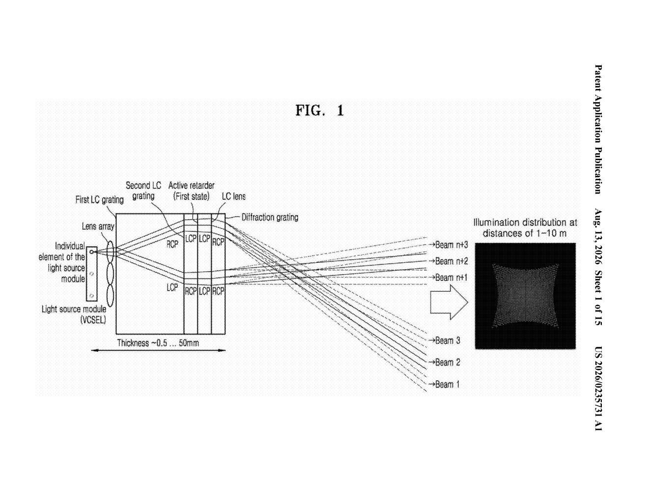
How LC gratings and a retarder flip between two light modes
The system sits in front of an infrared light source and manipulates the light using three main components arranged in sequence:
- LC gratings (liquid crystal diffraction gratings): These split the incoming unpolarized light into two separate beams, giving each beam a different circular polarization (think of polarization as the direction light waves spin as they travel). The two beams travel different spatial paths.
- Active retarder: A voltage-controlled liquid crystal layer that can flip the polarization of each beam to its opposite. This flip is what chooses the mode. When the retarder is active, one beam's polarization is reversed; when it is inactive, the beams stay as they are.
- LC lens: A liquid crystal lens that behaves very differently depending on polarization. For one polarization it has positive optical power (converges light into discrete dots), and for the orthogonal polarization it has negative optical power (spreads light into a continuous flood). Because the retarder controls which polarization reaches the lens in which state, toggling the retarder's voltage selects between dot-grid mode and flood mode.
The result is a single optical stack that produces a point illumination pattern (structured dots for face ID or precise depth mapping) or a flood illumination pattern (a solid light patch for face unlock in low light or quick ranging) with no mechanical movement whatsoever.
… according to the spot illumination mode, a point illumination pattern including a plurality of point illumination spots is generated on a surface of an illuminated object, and according to the flood illumination mode, a continuous illuminated spot is generated on the surface of the illuminated object …
Translation: The device can project either a grid of tiny dots to measure depth or a single broad light to capture a full image.
What this means for phone cameras that measure distance
Time-of-flight cameras already appear in flagship phones for portrait mode, face unlock, and AR effects, but current modules often pair separate emitters or fixed lenses for each mode, adding thickness and cost. A single module that handles both jobs electrically could let phone makers shrink the camera bar or free up space for other components. It also removes a mechanical failure point.
The broader push to make depth sensors thinner and more capable without adding bulk is a consistent thread in phone camera development, and this filing sits squarely in that race. Samsung's approach here is fairly specific to the combination of LC gratings, an active retarder, and a polarization-sensitive LC lens, which means any competitor who wants the same electrical switching trick needs to find a different optical path or license the idea. Patentlyze tracks new Big Tech patents across depth-sensing and AR optics where this kind of liquid crystal miniaturization is showing up more frequently as the industry chases thinner hardware.
Claim 1 is built around a specific, tightly defined combination: LC gratings that split by polarization, an active retarder that flips polarization state, and a polarization-sensitive LC lens that presents opposite optical powers to the two beams. That combination is narrow enough to be potentially defensible but broad enough to cover any phone or AR headset illuminator that achieves electrical mode-switching by this polarization-routing path. If granted, it would push competitors to reroute light differently (perhaps using MEMS mirrors or separate emitters) to achieve the same two-mode output, which adds cost or bulk. For a company as deep in phone hardware as Samsung, owning this mechanism could matter for Galaxy phones and for licensing leverage in the growing depth-sensor supply chain.
There are more where this came from
We read every patent application Big Tech publishes and send you the ones worth knowing. Plain English, free, every week.
The drawings
15 drawing sheets from US 2026/0235731 A1 · click any drawing to enlarge


Want this weekly breakdown for a company we don't cover? Patentlyze Pro →
Be the first to weigh in