
Sony Patents a Microscopic Metal Shell Surface That Controls Light Color by Design
Sony is patenting a way to build surfaces out of millions of microscopic hollow metal shells, each tuned to interact with a precise color of light. It's an approach that could reshape how camera sensors and optical filters are made at the hardware level.
What Sony's hollow metal nanostructure surface actually does
Ever tried to separate one specific color of light from a jumble of others, the way a prism splits sunlight into a rainbow? Optical engineers do this constantly, and it's harder than it sounds when you need it to happen at the microscopic scale inside a camera or a screen.
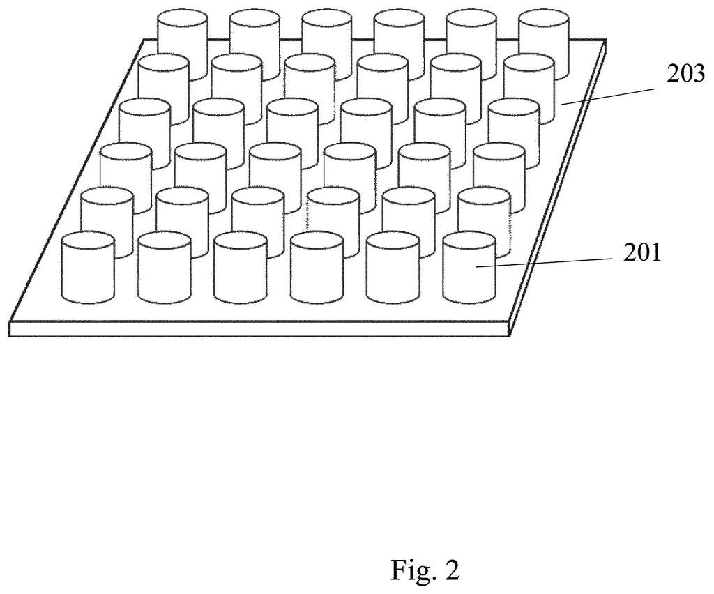
Sony's patent describes a surface covered in an enormous number of tiny structures, each one a hollow shape coated in an extremely thin layer of metal. The metal isn't solid all the way through; it's more like a shell. Because of the way light interacts with metal at very small scales, each shell can be tuned to resonate with, meaning amplify or filter, a specific color depending on its size and shape.
Plasmonic metasurfaces like this one let engineers design exactly which wavelengths of light a surface responds to, instead of relying on bulkier traditional optical components like lenses or filters. For you, that could eventually translate into thinner, more accurate sensors in cameras or medical imaging devices.
… a nanostructured dielectric component and at least one ultrathin metal layer of one or more plasmonic metals conformal to the nanostructure to define resonances at designed wavelengths.
Translation: A microscopic patterned base wrapped in an extremely thin metal layer that shapes light colors precisely.
How ultrathin metal shells lock onto specific light wavelengths
The patent describes a plasmonic metasurface: a flat surface engineered at the nanoscale to manipulate light in ways that ordinary materials cannot. "Plasmonic" refers to the behavior of electrons in a metal when they're hit by light at the right frequency; they oscillate in waves called plasmons, and those oscillations can absorb, concentrate, or redirect light with great precision.
The surface is built from a large number of identical or varied metaatoms (think of them as the individual repeating units that give the whole surface its optical properties). Each metaatom is a nanostructured dielectric shape, essentially a microscopic scaffold made of a non-conducting material, coated conformally with at least one ultrathin metal layer. "Conformal" means the metal follows every contour of the scaffold, like spray-painting a tiny sculpture rather than filling it solid.
Because the metal shell is hollow rather than solid, the resonance it creates (the specific wavelength of light it interacts with) can be tuned more precisely and with less material. The key parameters are:
- The geometry of the dielectric scaffold underneath
- The thickness of the metal coating
- The choice of plasmonic metal (typically gold, silver, or aluminum)
By varying those parameters across the surface, engineers can design a single flat layer that sorts, amplifies, or blocks multiple specific colors of light simultaneously, without the bulk of a traditional lens or filter stack.
What this means for future Sony camera sensors and displays
For camera sensors, the ability to filter or enhance particular wavelengths of light at the hardware level, inside a flat nanoscale coating rather than a stack of glass filters, opens a path to thinner and more sensitive imaging components. That matters most in applications where size is constrained: think smartphone cameras, endoscopes, or satellite sensors.
Sony Semiconductor Solutions' steady investment in advanced imaging materials suggests the company is building toward sensors that do more optical processing before the signal ever reaches the electronics. Whether this metasurface approach makes it into a shipping product depends on manufacturing yield at scale, which patents don't address. But the direction, replacing bulky optics with engineered flat surfaces, is one the imaging industry has been moving toward for several years.
This is the 62nd Sony filing we've tracked in our camera patents coverage since May, a topic that includes one using AI and invisible light and one for medical camera brightness.
This patent sits squarely in foundational materials research, the kind that rarely shows up in a product announcement for years, if ever. The gap between "we can tune a metasurface in a lab" and "we can manufacture a billion of these reliably" is large, and nothing here closes it.
That said, for anyone who uses a Sony camera or a Sony-sensored device, the payoff this points toward is real: optical filtering done by a coated surface instead of a glass sandwich means thinner modules and potentially better signal before any digital processing starts. That's a concrete benefit, not an abstract one.
The filing is specific enough to suggest Sony's semiconductor team is doing active experimental work here, not just staking legal territory. Whether you'd ever notice it depends entirely on whether the manufacturing problem gets solved.
There are more where this came from
We read every patent application Big Tech publishes and send you the ones worth knowing. Plain English, free, every week.
The drawings
11 drawing sheets from US 2026/0267039 A1 · click any drawing to enlarge


Want this weekly breakdown for a company we don't cover? Patentlyze Pro →