
Sony Patent Introduces Deliberate Air Gap to Reshape Surface-Emitting Laser Design
Sony is patenting a structural tweak inside vertical laser chips, a deliberate sliver of air, that could improve how tightly and efficiently they emit light. It sounds like a minor detail, but in laser physics, tiny geometry changes have outsized effects.
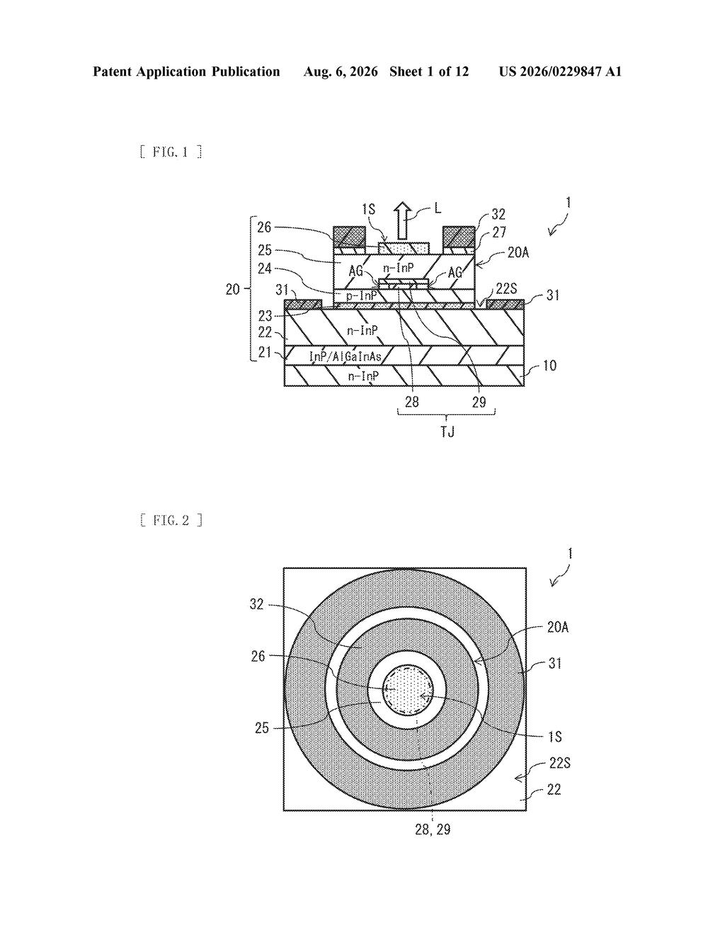
What Sony's air-gap laser design actually changes
Imagine a tiny laser, smaller than a grain of sand, built like a sandwich of ultra-thin layers. These lasers are everywhere: they're inside the face-unlock sensors on your phone, the depth cameras on robots, and the LiDAR systems in self-driving cars.
Sony's patent describes a specific structural change to one of these lasers, called a VCSEL (a vertical laser that shoots light straight up through its top surface). Instead of packing all the internal layers tightly together, Sony's design leaves a deliberate air gap between one layer and the side of a component called the tunnel junction. That gap changes how the light bounces and focuses inside the device.
The practical idea is that this air gap acts as a kind of optical fence, keeping the light better confined to the center of the laser. Better confinement generally means a cleaner, more efficient beam. For Sony, which makes image sensors and laser components used in phones and cameras, getting more out of each laser chip matters.
… a tunnel junction layer disposed between the active layer and the second DBR layer, and surrounded by the second spacer layer, wherein the second spacer layer and a portion of a side surface of the tunnel junction layer have an air gap therebetween.
Translation: A tiny pocket of air sits right next to the tunnel junction layer inside the laser.
How the air gap sits inside the laser stack
The patent describes a VCSEL (Vertical-Cavity Surface-Emitting Laser), a type of semiconductor laser that emits light perpendicular to its top surface rather than out the side. VCSELs are built as stacks of ultra-thin semiconductor layers, and their performance depends heavily on the precise geometry of those layers.
The key innovation here is the placement of an air gap between the second spacer layer and part of the side surface of the tunnel junction layer. A tunnel junction (a thin semiconductor sandwich that lets electrons tunnel through quantum-mechanically, boosting current efficiency) normally sits surrounded by other solid material. Sony's design intentionally leaves a void there instead.
Why does that matter? Air has a very different refractive index (the measure of how much it bends or reflects light) compared to semiconductor materials. Placing air next to the side of the tunnel junction creates a sharp optical boundary that helps confine the laser light more tightly to the vertical center of the device. This is sometimes called index guiding.
- Better optical confinement can reduce threshold current (the minimum power needed to start lasing)
- It can improve beam quality and reduce unwanted side modes
- The design also affects thermal behavior, since air is a poor conductor of heat
The second spacer layer is disposed between the active layer and the second DBR layer. The tunnel junction layer is disposed between the active layer and the second DBR layer, and is surrounded by the second spacer layer.
Translation: A special layer that handles electrical current is tucked right between the main light-producing active layer and the top mirror.
What this means for sensors, cameras, and LiDAR
VCSELs are already inside hundreds of millions of consumer devices, and Sony is one of the largest suppliers of image sensors and optical components globally. Even incremental gains in laser efficiency or beam quality translate directly into longer battery life, better depth-sensing accuracy, and cheaper manufacturing at scale.
The patent also covers arrays of these lasers, not just single emitters. That points toward applications like 3D sensing modules and LiDAR, where dozens or hundreds of VCSELs fire together. If Sony can make each emitter in an array perform more consistently, the whole system benefits. For consumers, that could eventually show up as more accurate face unlock, better low-light camera depth maps, or more reliable proximity sensors.
This is a focused, incremental engineering patent rather than a sweeping technology claim. The air-gap trick is a real structural idea with grounding in established laser physics, and Sony has the manufacturing capability to actually implement it. It won't make headlines outside of photonics circles, but it's the kind of quiet refinement that keeps Sony's component business competitive.
There are more where this came from
We read every patent application Big Tech publishes and send you the ones worth knowing. Plain English, free, every week.
The drawings
12 drawing sheets from US 2026/0229847 A1 · click any drawing to enlarge


Want this weekly breakdown for a company we don't cover? Patentlyze Pro →
Be the first to weigh in