
Sony Patent Stacks Three Chips to Shrink Distance-Sensing Camera Designs
Sony has filed a patent for a distance sensor that squeezes three specialized chips into one compact stack, potentially making the kind of depth-sensing hardware found in cameras and robotics much smaller than it is today.
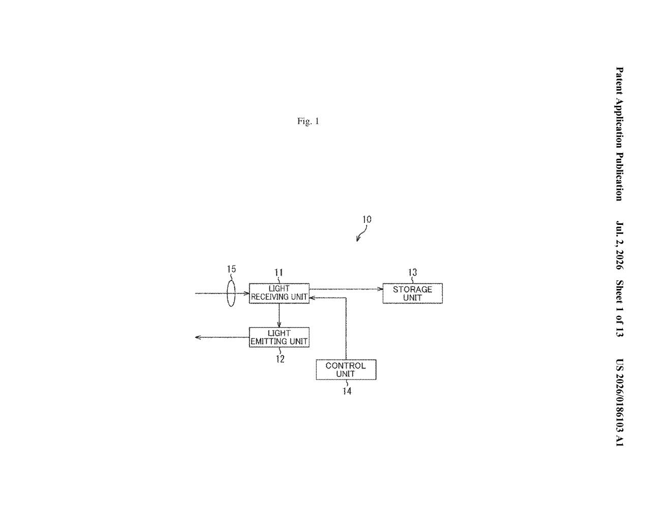
What Sony's three-chip distance sensor actually does
Imagine your phone's camera trying to figure out how far away your face is before unlocking. To do that, it needs to fire a pulse of light, catch the light that bounces back, and then crunch numbers to calculate the distance. Today, doing all three of those jobs in a tiny device requires a lot of space.
Sony's patent describes a way to split that work across three specialized chips, then stack them on top of each other like a very small layer cake. One chip handles shooting the light, one handles catching it and doing initial processing, and a third chip sits underneath both, acting as the brain that coordinates everything.
By connecting each chip directly on top of the shared base chip, rather than running long wires between separate components on a circuit board, the whole assembly gets dramatically smaller. That kind of miniaturization matters most in places where space is tight: smartphones, AR glasses, drones, or medical imaging tools.
How the three chips divide the sensing workload
The patent describes a distance measuring device built from three distinct semiconductor chips, each assigned a specific role:
- Chip one contains the light emitting elements, the components that fire pulses of light (typically infrared) toward whatever object is being measured.
- Chip two is itself a two-layer stack: a top layer holds the light receiving elements (think of them as tiny sensors that detect returning light), and a bottom layer holds the first round of signal processing circuitry that converts those light signals into pixel data.
- Chip three is the control hub: it manages when and how chip one fires its light, and it handles the deeper signal processing from chip two to actually calculate distance.
The key engineering detail is how chips one and two are connected to chip three. The patent uses chip-on-chip bonding, meaning each chip is mounted directly on the surface of chip three using microscopic electrical contacts rather than routed through a larger circuit board. This eliminates the need for long signal traces between components, which saves physical space and can reduce signal delay.
The result is a self-contained sensor module that is meaningfully smaller than a traditional multi-chip design laid out side by side on a board.
What this means for cameras and depth-sensing devices
Distance sensing, sometimes called depth sensing or LiDAR at the consumer level, already shows up in your smartphone's Face ID, in robot vacuum navigation, in automotive safety systems, and in augmented reality headsets. The limiting factor for putting better depth sensors into more devices is often physical size. A smaller sensor module means it can fit into thinner phones, smaller wearables, or cheaper industrial cameras without sacrificing sensing capability.
Sony is one of the world's largest image sensor manufacturers, supplying chips to Apple, Samsung, and many camera brands. A miniaturized distance sensor built around this stacked architecture could eventually appear across a wide range of consumer and industrial products, though a patent filing does not guarantee a shipping product.
This is a solid, workmanlike engineering patent rather than a conceptual moonshot. Sony is one of the few companies in the world that actually manufactures image sensors at scale, so a filing like this is more likely than most to eventually become a real product. The three-chip stacking approach is a logical evolution of the same multi-layer chip designs Sony already uses in its image sensors, which makes this feel like incremental but meaningful progress.
Get our take in your Top Stories
Liked this breakdown? Add Patentlyze as a preferred source on Google, and our plain-English take shows up more often in your Top Stories the next time Sony patent news breaks.
There are more where this came from
We read every patent application Big Tech publishes and send you the ones worth knowing. Plain English, free, every week.
Want this weekly breakdown for a company we don't cover? Patentlyze Pro →