Samsung Patents a Higher-Melting-Point Solder Guard for Chip Packages
Solder bumps are one of the most failure-prone parts of a chip package — they melt, crack, and oxidize under heat. Samsung's new patent puts a metal shield around each bump that deliberately melts at a higher temperature than the bump itself.
What Samsung's solder bump protection layer actually does
Imagine the tiny metallic dots that connect a chip to its circuit board. Those dots — called solder bumps — have to survive extreme heat during manufacturing and then stay intact for years of use. The problem is that they're made of tin-based solder, which melts at a relatively low temperature and can degrade or short-circuit if anything goes wrong.
Samsung's patent describes wrapping each solder bump in a thin metal protection layer that's also tin-based — but engineered to have a higher melting point than the bump underneath. Think of it like a heat-resistant jacket around a more fragile core.
The idea is that during reflow soldering (when heat is applied to bond chips together), the outer shell stays solid while the inner bump does the melting and bonding work. That outer layer protects against oxidation and physical damage, potentially making the whole package more reliable and easier to manufacture without defects.
How the tin protection layer raises the melting threshold
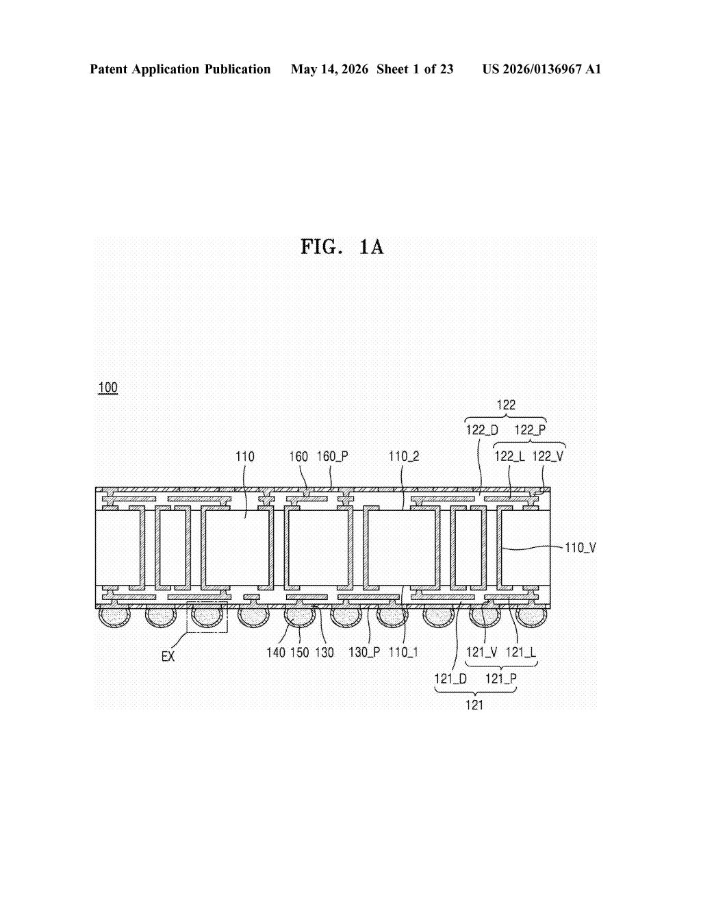
The patent describes a package substrate — essentially the layered circuit board that a chip sits on — with a specific structure around its solder connection points.
At the heart of it is a layered stack:
- A base layer with internal wiring channels called through vias (vertical tunnels that carry signals from one side of the substrate to the other)
- A distribution structure — fine patterned wiring layers — on top of the base
- Bump pads, which are the landing zones where solder attaches
- Connection terminals (the solder bumps themselves), made of tin (Sn) with a melting point at "first temperature"
- A metal protection layer on the surface of each connection terminal, also containing Sn, but formulated to melt at a higher "second temperature"
The critical claim is that the protection layer's melting point exceeds the solder bump's. This means during assembly, when heat is applied, the inner bump flows and bonds as intended while the outer shell remains structurally intact. A passivation layer (an insulating barrier that prevents electrical leakage) surrounds each bump pad and keeps the terminals electrically isolated from each other.
The specific tin-based chemistry of the protection layer is left somewhat open in the claim, but the melting-point differential is the patentable core of the idea.
What this means for advanced semiconductor packaging reliability
Solder joint reliability is one of the unglamorous bottlenecks in high-density chip packaging — especially as advanced packages stack more dies closer together and run hotter. A protection layer that guards against oxidation and reflow damage without requiring exotic materials could meaningfully improve yield rates in manufacturing, which directly affects cost.
For Samsung, which competes aggressively in both memory packaging (HBM) and advanced foundry services, incremental reliability improvements at the substrate level add up. This kind of patent is the infrastructure work that rarely makes headlines but quietly shows up in shipping products. It's not flashy, but it's the sort of detail that separates high-volume packaging yields from chronic defect problems.
This is a focused, incremental materials engineering patent — not a concept play. The melting-point differential between a solder bump and its protective shell is a real and practical problem in chip packaging, and Samsung is staking a claim on a specific tin-based solution. It won't rewrite the industry, but it's the kind of IP that quietly accumulates into a packaging technology moat.
Get one Big Tech patent every Sunday
Plain English, intelligent commentary, no hype. Free.
Editorial commentary on a publicly published patent application. Not legal advice.