
Samsung
Samsung · Display · Filed Nov 7, 2025 · USPTO published May 14, 2026 · May 14 release
Samsung Display Patents a Precise Quantum Dot Shell-Coating Method for Displays
The difference between a vivid, accurate color on your TV and a washed-out one can come down to a few nanometers of shell coating on a quantum dot. Samsung Display is patenting a tightly controlled recipe for building those shells — and the order of ingredients turns out to matter a lot.
- Publication number
- US 2026/0132331 A1(US20260132331A1)
- Applicant
- Samsung Display Co., Ltd.
- Filed · Published
- Nov 7, 2025 · May 14, 2026
- Inventors
- Junehyuk Jung, Sungjae Kim, Youngsik Kim, Hongrae Kim, Seungwon Park, Bitna Yoon, Taekjoon Lee
- Status when we published
- Waiting for an examiner
- Document
- 20 claims
- US classification
- 257/79
What Samsung's layered quantum dot recipe actually does
Imagine making a jawbreaker candy, but at the atomic scale. The hard center needs a perfectly even coating — put the wrong layer on first, or add ingredients out of order, and the whole thing falls apart. That's essentially the challenge Samsung Display is solving here with quantum dots.
Quantum dots are tiny semiconductor crystals — we're talking just a few nanometers wide — that glow a very precise color when hit with light. They're already inside many high-end TVs and monitors to produce richer, more accurate colors. But their performance depends heavily on how well a protective shell is grown around the crystal core.
Samsung's patent describes a specific step-by-step method for growing that shell: first you mix the core crystal with one type of chemical precursor, then you add a second. That sequence — not just the ingredients, but the order — is what Samsung is claiming as their innovation here.
How Samsung sequences the shell precursor additions
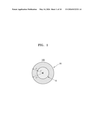
The patent covers a two-stage shell synthesis method for quantum dots built around a copper-containing core. Specifically, the core is made of copper (Cu), a Group III element (like indium or gallium), and a Group VI element (like sulfur or selenium) — a class of materials sometimes called I-III-VI quantum dots, which are considered more environmentally friendly than cadmium-based alternatives.
The key innovation is in how the first shell gets grown around that core. Rather than adding both shell-forming chemicals at once, Samsung's method splits it into two compositions:
- First composition: the core is mixed with a Group VI element-containing precursor (the sulfur or selenium source) first.
- Second composition: only then is a Group II element-containing precursor (think zinc) added to the mix.
This sequential addition — chalcogen first, then the metal — is likely designed to control how the shell nucleates and grows at the atomic level. In quantum dot chemistry, premature reactions between precursors can cause defects at the core-shell interface, which scatter light and reduce the quantum yield (basically, how efficiently the dot converts one color of light into another).
A second shell layer is also referenced in the broader patent, suggesting a multi-shell architecture aimed at further passivating (sealing off) surface defects that would otherwise cause the dot to lose energy as heat rather than light.
What this means for Samsung's next QLED and QD-OLED panels
For Samsung Display, quantum dot purity and consistency is a direct competitive lever. Their QD-OLED panels — used in products like the Odyssey monitors and high-end TVs — already use quantum dot color conversion layers. Any improvement in quantum yield or color stability translates into panels that are brighter, more color-accurate, or more power-efficient. Even small gains at the materials level compound into meaningful product differentiation.
The move toward cadmium-free quantum dots (which is what copper-based I-III-VI dots represent) is also worth noting. EU RoHS regulations restrict cadmium in consumer electronics, so Samsung has strong regulatory pressure to perfect the chemistry of greener alternatives. This patent suggests they're investing seriously in making those alternatives perform just as well as the cadmium-based dots they'd replace.
Source: US 2026/0132331 A1 at the USPTO (PDF). Full patent text and figures are in the official publication.
Get our take in your Top Stories
Liked this breakdown? Add Patentlyze as a preferred source on Google, and our plain-English take shows up more often in your Top Stories the next time Samsung patent news breaks.
Add Patentlyze on Google
One click.
There are more where this came from
We read every patent application Big Tech publishes and send you the ones worth knowing. Plain English, free, every week.
More from Samsung
All 1,629 Samsung patents →
More in Display
All 736 Display patents →
Sony
New Sony Patent Corrects Blurry Edges So Cameras Detect Fast Movement More Accurately
Intel
Intel Patents Technology That Resizes Screen Content Based on Your Distance
Apple
Folded Laser Beam Patent Could Shrink Gadgets That Measure Distance
Intel