Samsung Patents a Chip Component That Runs Its Own Internal Diagnostic Tests
Samsung has filed a patent for a multi-chip package design where one of the chips essentially doubles as a test wire — routing diagnostic signals through its own internal circuitry so engineers can verify the whole assembly is working before it ever ships.
What Samsung's self-testing chip package actually does
Imagine buying a piece of furniture that came with a hidden built-in tool to check whether every screw was seated correctly before you left the warehouse. That's roughly the idea here.
Samsung's patent covers a chip package — the sealed unit that holds one or more computer chips together on a small board — that has a clever way of checking its own connections. Instead of needing extra external probes or test hardware, two or more of the tiny metal bumps that connect a chip to the board are wired together through the chip itself. Engineers can send a signal in one bump and check whether it comes out the other, confirming the joints are solid.
The design puts two chips side by side on the same board, with the "test" chip handling that loopback job while still allowing normal data connections to reach the outside world through separate bumps. It's a quality-control trick baked into the physical structure of the package itself.
How the on-chip connection line loops test signals
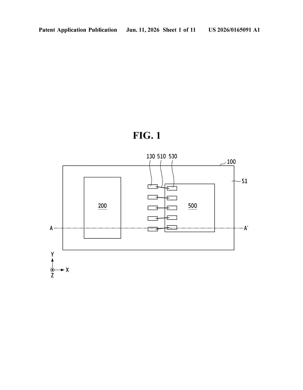
The patent describes a semiconductor package — a self-contained assembly of chips, a small substrate (think a mini circuit board), and the metal connections that tie them together.
The substrate has two sides. The bottom side (first surface) carries external connection terminals — the solder balls you'd find on a chip meant to attach to a larger motherboard — plus dedicated test pads that are physically separated from those live terminals. The top side (second surface) hosts two chips sitting side by side.
The first chip is where the testing magic happens. It contains an on-chip connection line — an internal wire loop that links at least two of the metal bumps sitting beneath it. Those bumps are called test bumps. When a test signal enters one bump, it travels up into the chip, across the on-chip line, and back down through another bump, completing a loop. A separate set of bumps — the connection bumps — carries real data and is wired through the substrate to the external terminals on the bottom.
The second chip sits alongside the first, also on the top surface. The patent doesn't specify its function in detail, but its presence confirms this is a multi-chip module design, the kind used in high-bandwidth memory stacks and advanced AI accelerator packages.
What this means for chip defect detection in production
Catching a bad solder joint or a misaligned bump after a chip is fully assembled and sealed is expensive — often the whole package is scrapped. By routing test signals through the chip's own internal wiring, Samsung's design lets manufacturers run continuity checks at the package level without extra test hardware touching the live signal pins. That keeps production yields up and defect-escape rates down.
This kind of built-in testability is increasingly important as chip packages grow more complex — stacking memory, logic, and specialty chips into a single unit. If this approach makes it into Samsung's high-volume packaging lines, it could quietly reduce the cost of the advanced packages used in AI chips, smartphone processors, and server memory.
This is unglamorous but genuinely useful manufacturing engineering. Built-in loopback testing at the package level is a real cost-saver in high-volume semiconductor production, and Samsung filing this now — while multi-chip packaging is exploding in AI hardware — is well-timed. Don't expect a press release, but do expect this kind of design to quietly show up in future package specs.
Get one Big Tech patent every Sunday
Plain English, intelligent commentary, no hype. Free.
Editorial commentary on a publicly published patent application. Not legal advice.